This thread has been locked.

If you have a related question, please click the "Ask a related question" button in the top right corner. The newly created question will be automatically linked to this question.

LMX2594: Software sync - how it works?

Part Number: LMX2594

Hello guys, i have several questions regarding the  sync option of LMX2594.

1.How exactly the software sync works? In the datasheet the info is quite contradictory: page 29 of datasheet SNAS696C–MARCH2017–REVISEDAPRIL2019:

firstly, in point 5:

-you have to program the device with the VCO_PHASE_SYNC=1, which "that this does not count as applying a SYNC to device (for category2).

And  next, in point 6:

-Apply the SYNC,if required:1. If category 2, VCO_PHASE_SYNC can be toggled from 0 to 1. 

So , how  can I toggle the pin from 0 to 1, if it's already programmed in 1 on the previous step?

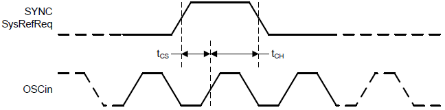
2. And another question regarding the timing requirements for SYNC pulse. It looks that the SYNC with hardware pin is not always successful. So, please, explain the requirements in the table on page 11.

How can obtain a feedback from the sync procedure?

3. Is there an option to mute te RFout outputs, if the device is not locked to the RefOsc signal? I saw there is an option to be muted during the calibration, but i could not find a way to set the registers for auto mute it if it's not locked?

Will be waiting for a response!

  • Hi Lyubomir,

    For cat. 2, here is the programming sequence:

    1. Setup as usual.
    2. Program all the registers as usual. The device is now locked.
    3. Program N = N' / IncludeDivide, where N' is the original N divider and fraction values you used in step 2.
    4. Program R0 with VCO_PHASE_SYNC = 1.
    5. Program N = N'.
    6. Program R0 with VCO_PHASE_SYNC = 0.
    7. Alternatively, step 3 to 6 can be replaced by applying a SYNC signal (0 → 1 transition) to the SYNC pin and the timing on this in not critical.

    The programming sequence for cat. 3 is as follows:

    1. Ensure that the maximum fOSCin for SYNC is not violated and there are hardware accommodations to use the SYNC pin.
    2. If neither OUTA_MUX nor OUTB_MUX is equal to 0 (Channel divider output), program N divider as usual.
    3. If one of the OUTA_MUX or OUTB_MUX is equal to 1, set N = N' / IncludeDivide, where N' is the normal N divider (integer + fraction) value.
    4. Program all the registers with R0 VCO_PHASE_SYNC = 1.
    5. Apply a SYNC signal (0 → 1 transition) to the SYNC pin. The timing of the SYNC signal as shown in datasheet section 6.6 is critical.

    The hardware does not support auto-mute for lock status. But you could read back R110[10:9] (or detect MUXout) for lock status and then program OUTA_PD to mute the output.

  • Hello Noel,

    thank you for the reply. I cannot find in the datasheet, sec 6.6 time requirements for sync signal? Which version of the datasheet i have to look at? What is Tsc, Tch ?

    According to auto-mute function when the PLL is not locked; yes, i can do it with external MCU, but it's slower and not so reliable option, As far as the PLL is used for upstreaming, timing could be critical.

    Regards,

    Lyubomir

  • Hi Lyubomir,

    I borrowed the picture from another datasheet, tCS and tCH are referring to the setup and hold time of section 6.6.