This thread has been locked.

If you have a related question, please click the "Ask a related question" button in the top right corner. The newly created question will be automatically linked to this question.

LMK04832: No SYSREF output on SCLKs

Part Number: LMK04832
Other Parts Discussed in Thread: LMK04826

I'm working on migrating a design with an existing PCB from LMK04826B to LMK04832. The board was working properly prior to replacing the PLL. Our source code has been updated to match the changes in the register map of the PLL, but it looks like we've missed something as I'm not getting any SYSREF signal on any of the SCLK outputs.

Some troubleshooting I've attempted:

- Tried both continuous and pulser output from the SYSREF_MUX, neither shows up at the SCLK outputs
- Tried switching the SCLK outputs to device clock via the CLKoutY_SRC_MUX, which works fine and outputs a clock signal
- Tried toggling SCLKX_Y_POL for the SCLK output, which works and causes the output to toggle
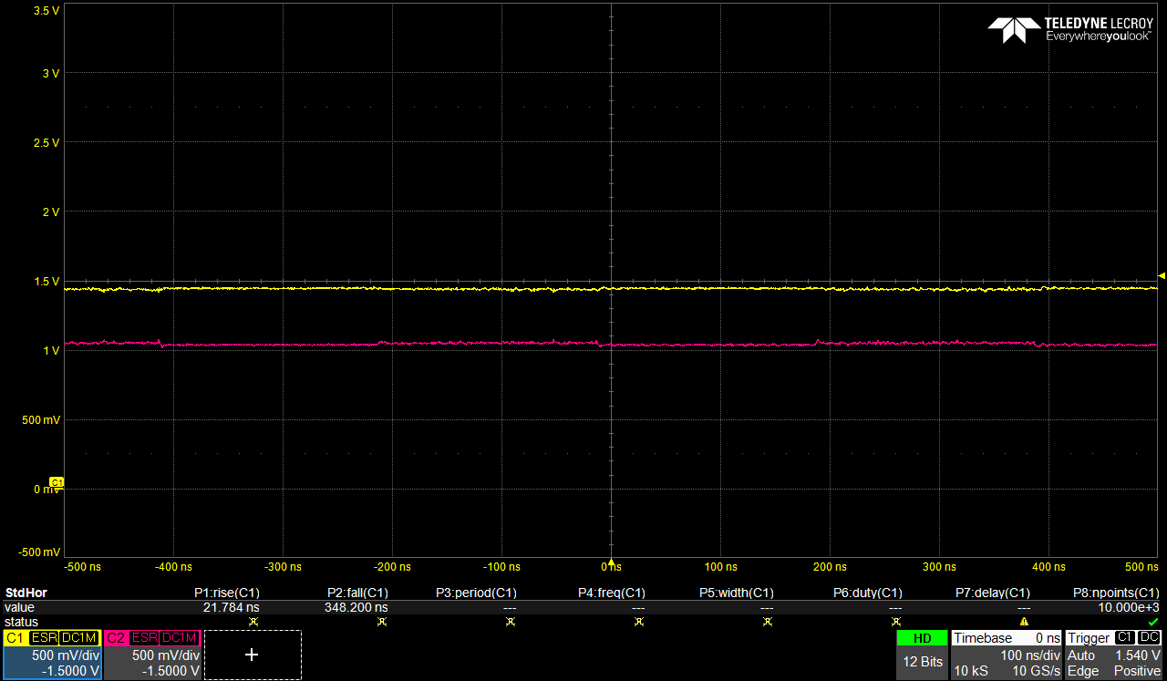
- Tried measuring the SYSREF_DIV clock via OSCout, using FB_MUX == SYSREF_DIV and OSCout_MUX == FB_MUX. This shows correct signal, 2.5 MHz with 50% duty cycle- Tried enabling/disabling parts of the SCLK signal path (DDLY, analog delay, etc), but none of the changes result in SYSREF output

Given that I've verified that SYSREF_DIV is OK via OSCout, and that the signal path from SCLKX_Y_POL and out to the PCB is OK by toggling the polarity, I'm assuming it must be something in between that stops the signal? SYSREF_CLR is zeroed when I'm doing these measurements.

The two PLLs both signal lock detect. I'm using a 10 MHz reference into PLL1, which controls a 100 MHz VCXO. PLL2 goes from 100 MHz to 2.5 GHz. PLL1 uses SYSREF_DIV as feedback, PLL2 uses local feedback via prescaler. SYSREF_DIV divides by 1000 to get 2.5 MHz. The outputs where I want SYSREF output are CLKout3, CLKout9 and CLKout13.

I've attached text files containing a readout of the register map, plus a parsed version where I've extracted the values of individual fields in the registers for easier reading.

0x000 0x10
0x001 0x00
0x002 0x00
0x003 0x06
0x004 0x63
0x005 0xD1
0x006 0x70
0x007 0x00
0x008 0x00
0x009 0x00
0x00A 0x00
0x00B 0x00
0x00C 0x51
0x00D 0x04
0x100 0x0A
0x101 0x00
0x102 0x00
0x103 0x00
0x104 0x34
0x105 0x00
0x106 0x08
0x107 0x01
0x108 0x08
0x109 0x00
0x10A 0x00
0x10B 0x00
0x10C 0x20
0x10D 0x00
0x10E 0x08
0x10F 0x11
0x110 0x08
0x111 0x00
0x112 0x00
0x113 0x00
0x114 0x10
0x115 0x00
0x116 0x08
0x117 0x11
0x118 0xFA
0x119 0x00
0x11A 0x00
0x11B 0x00
0x11C 0x34
0x11D 0x00
0x11E 0x08
0x11F 0x01
0x120 0x01
0x121 0x00
0x122 0x60
0x123 0x00
0x124 0x20
0x125 0x00
0x126 0x08
0x127 0x44
0x128 0x08
0x129 0x0A
0x12A 0x80
0x12B 0x50
0x12C 0x10
0x12D 0x00
0x12E 0x01
0x12F 0x00
0x130 0x01
0x131 0x00
0x132 0x60
0x133 0x00
0x134 0x20
0x135 0x00
0x136 0x08
0x137 0x44
0x138 0x18
0x139 0x03
0x13A 0x03
0x13B 0xE8
0x13C 0x00
0x13D 0x08
0x13E 0x00
0x13F 0x0D
0x140 0x00
0x141 0x80
0x142 0x00
0x143 0x50
0x144 0xFF
0x145 0x00
0x146 0x00
0x147 0x1A
0x148 0x0B
0x149 0x0B
0x14A 0x02
0x14B 0x16
0x14C 0x00
0x14D 0x00
0x14E 0x00
0x14F 0x7F
0x150 0x09
0x151 0x02
0x152 0x00
0x153 0x00
0x154 0x04
0x155 0x00
0x156 0x04
0x157 0x00
0x158 0x96
0x159 0x00
0x15A 0x01
0x15B 0x14
0x15C 0x3F
0x15D 0xFF
0x15E 0x1E
0x15F 0x3B
0x160 0x00
0x161 0x01
0x162 0xA4
0x163 0x00
0x164 0x00
0x165 0x05
0x166 0x00
0x167 0x00
0x168 0x05
0x169 0x59
0x16A 0x3F
0x16B 0xFF
0x16C 0x00
0x16D 0x00
0x16E 0x06
0x16F 0x20
0x170 0xA8
0x171 0xAA
0x172 0x02
0x173 0x0F
0x174 0x00
0x175 0x00
0x176 0x00
0x177 0x00
0x178 0x40
0x179 0x00
0x17A 0x18
0x17B 0x77
0x17C 0x15
0x17D 0x33
0x17E 0x00
0x17F 0x05
0x180 0x80
0x181 0x00
0x182 0x00
0x183 0x05
0x184 0x50
0x185 0xAF
0x186 0x00
0x187 0x00
0x188 0x41

Register 0x100 = 0x0A
        DCLK0_1_DIV[7:0]   10

Register 0x101 = 0x00
       DCLK0_1_DDLY[7:0]   0

Register 0x102 = 0x00
            CLKout0_1_PD   0
           CLKout0_1_ODL   0
           CLKout0_1_IDL   0
         DCLK0_1_DDLY_PD   0
       DCLK0_1_DDLY[9:8]   0
        DCLK0_1_DIV[9:8]   0

Register 0x103 = 0x00
           Reserved == 1   0
         CLKout0_SRC_MUX   0  == Device Clock
              DCLK0_1_PD   0
             DCLK0_1_BYP   0
             DCLK0_1_DCC   0
             DCLK0_1_POL   0
              DCLK0_1_HS   0

Register 0x104 = 0x34
         CLKout1_SRC_MUX   1  == SYSREF
              SCLK0_1_PD   1
        SCLK0_1_DIS_MODE   1
             SCLK0_1_POL   0
              SCLK0_1_HS   0

Register 0x105 = 0x00
         SCLK0_1_ADLY_EN   0
            SCLK0_1_ADLY   0

Register 0x106 = 0x08
            SCLK0_1_DDLY   8

Register 0x107 = 0x01
             CLKout1_FMT   0
             CLKout0_FMT   1

Register 0x108 = 0x08
        DCLK2_3_DIV[7:0]   8

Register 0x109 = 0x00
       DCLK2_3_DDLY[7:0]   0

Register 0x10A = 0x00
            CLKout2_3_PD   0
           CLKout2_3_ODL   0
           CLKout2_3_IDL   0
         DCLK2_3_DDLY_PD   0
       DCLK2_3_DDLY[9:8]   0
        DCLK2_3_DIV[9:8]   0

Register 0x10B = 0x00
           Reserved == 1   0
         CLKout2_SRC_MUX   0  == Device Clock
              DCLK2_3_PD   0
             DCLK2_3_BYP   0
             DCLK2_3_DCC   0
             DCLK2_3_POL   0
              DCLK2_3_HS   0

Register 0x10C = 0x20
         CLKout3_SRC_MUX   1  == SYSREF
              SCLK2_3_PD   0
        SCLK2_3_DIS_MODE   0
             SCLK2_3_POL   0
              SCLK2_3_HS   0

Register 0x10D = 0x00
         SCLK2_3_ADLY_EN   0
            SCLK2_3_ADLY   0

Register 0x10E = 0x08
            SCLK2_3_DDLY   8

Register 0x10F = 0x11
             CLKout3_FMT   1
             CLKout2_FMT   1

Register 0x110 = 0x08
        DCLK4_5_DIV[7:0]   8

Register 0x111 = 0x00
       DCLK4_5_DDLY[7:0]   0

Register 0x112 = 0x00
            CLKout4_5_PD   0
           CLKout4_5_ODL   0
           CLKout4_5_IDL   0
         DCLK4_5_DDLY_PD   0
       DCLK4_5_DDLY[9:8]   0
        DCLK4_5_DIV[9:8]   0

Register 0x113 = 0x00
           Reserved == 1   0
         CLKout4_SRC_MUX   0  == Device Clock
              DCLK4_5_PD   0
             DCLK4_5_BYP   0
             DCLK4_5_DCC   0
             DCLK4_5_POL   0
              DCLK4_5_HS   0

Register 0x114 = 0x10
         CLKout5_SRC_MUX   0  == Device Clock
              SCLK4_5_PD   1
        SCLK4_5_DIS_MODE   0
             SCLK4_5_POL   0
              SCLK4_5_HS   0

Register 0x115 = 0x00
         SCLK4_5_ADLY_EN   0
            SCLK4_5_ADLY   0

Register 0x116 = 0x08
            SCLK4_5_DDLY   8

Register 0x117 = 0x11
             CLKout5_FMT   1
             CLKout4_FMT   1

Register 0x118 = 0xFA
        DCLK6_7_DIV[7:0]   250

Register 0x119 = 0x00
       DCLK6_7_DDLY[7:0]   0

Register 0x11A = 0x00
            CLKout6_7_PD   0
           CLKout6_7_ODL   0
           CLKout6_7_IDL   0
         DCLK6_7_DDLY_PD   0
       DCLK6_7_DDLY[9:8]   0
        DCLK6_7_DIV[9:8]   0

Register 0x11B = 0x00
           Reserved == 1   0
         CLKout6_SRC_MUX   0  == Device Clock
              DCLK6_7_PD   0
             DCLK6_7_BYP   0
             DCLK6_7_DCC   0
             DCLK6_7_POL   0
              DCLK6_7_HS   0

Register 0x11C = 0x34
         CLKout7_SRC_MUX   1  == SYSREF
              SCLK6_7_PD   1
        SCLK6_7_DIS_MODE   1
             SCLK6_7_POL   0
              SCLK6_7_HS   0

Register 0x11D = 0x00
         SCLK6_7_ADLY_EN   0
            SCLK6_7_ADLY   0

Register 0x11E = 0x08
            SCLK6_7_DDLY   8

Register 0x11F = 0x01
             CLKout7_FMT   0
             CLKout6_FMT   1

Register 0x120 = 0x01
        DCLK8_9_DIV[7:0]   1

Register 0x121 = 0x00
       DCLK8_9_DDLY[7:0]   0

Register 0x122 = 0x60
            CLKout8_9_PD   0
           CLKout8_9_ODL   1
           CLKout8_9_IDL   1
         DCLK8_9_DDLY_PD   0
       DCLK8_9_DDLY[9:8]   0
        DCLK8_9_DIV[9:8]   0

Register 0x123 = 0x00
           Reserved == 1   0
         CLKout8_SRC_MUX   0  == Device Clock
              DCLK8_9_PD   0
             DCLK8_9_BYP   0
             DCLK8_9_DCC   0
             DCLK8_9_POL   0
              DCLK8_9_HS   0

Register 0x124 = 0x20
         CLKout9_SRC_MUX   1  == SYSREF
              SCLK8_9_PD   0
        SCLK8_9_DIS_MODE   0
             SCLK8_9_POL   0
              SCLK8_9_HS   0

Register 0x125 = 0x00
         SCLK8_9_ADLY_EN   0
            SCLK8_9_ADLY   0

Register 0x126 = 0x08
            SCLK8_9_DDLY   8

Register 0x127 = 0x44
             CLKout9_FMT   4
             CLKout8_FMT   4

Register 0x128 = 0x08
      DCLK10_11_DIV[7:0]   8

Register 0x129 = 0x0A
     DCLK10_11_DDLY[7:0]   10

Register 0x12A = 0x80
          CLKout10_11_PD   1
         CLKout10_11_ODL   0
         CLKout10_11_IDL   0
       DCLK10_11_DDLY_PD   0
     DCLK10_11_DDLY[9:8]   0
      DCLK10_11_DIV[9:8]   0

Register 0x12B = 0x50
           Reserved == 1   1
        CLKout10_SRC_MUX   0  == Device Clock
            DCLK10_11_PD   1
           DCLK10_11_BYP   0
           DCLK10_11_DCC   0
           DCLK10_11_POL   0
            DCLK10_11_HS   0

Register 0x12C = 0x10
        CLKout11_SRC_MUX   0  == Device Clock
            SCLK10_11_PD   1
      SCLK10_11_DIS_MODE   0
           SCLK10_11_POL   0
            SCLK10_11_HS   0

Register 0x12D = 0x00
       SCLK10_11_ADLY_EN   0
          SCLK10_11_ADLY   0

Register 0x12E = 0x01
          SCLK10_11_DDLY   1

Register 0x12F = 0x00
            CLKout11_FMT   0
            CLKout10_FMT   0

Register 0x130 = 0x01
      DCLK12_13_DIV[7:0]   1

Register 0x131 = 0x00
     DCLK12_13_DDLY[7:0]   0

Register 0x132 = 0x60
          CLKout12_13_PD   0
         CLKout12_13_ODL   1
         CLKout12_13_IDL   1
       DCLK12_13_DDLY_PD   0
     DCLK12_13_DDLY[9:8]   0
      DCLK12_13_DIV[9:8]   0

Register 0x133 = 0x00
           Reserved == 1   0
       CLKout132_SRC_MUX   0  == Device Clock
            DCLK12_13_PD   0
           DCLK12_13_BYP   0
           DCLK12_13_DCC   0
           DCLK12_13_POL   0
            DCLK12_13_HS   0

Register 0x134 = 0x20
        CLKout13_SRC_MUX   1  == SYSREF
            SCLK12_13_PD   0
      SCLK12_13_DIS_MODE   0
           SCLK12_13_POL   0
            SCLK12_13_HS   0

Register 0x135 = 0x00
       SCLK12_13_ADLY_EN   0
          SCLK12_13_ADLY   0

Register 0x136 = 0x08
          SCLK12_13_DDLY   8

Register 0x137 = 0x44
            CLKout13_FMT   4
            CLKout12_FMT   4

Register 0x138 = 0x18
                 VCO_MUX   0
              OSCout_MUX   1
              OSCout_FMT   8

Register 0x139 = 0x03
           SYSREF_REQ_EN   0
             SYNC_BYPASS   0
              SYSREF_MUX   3  == SYSREF continuous

Register 0x13A = 0x03
        SYSREF_DIV[12:8]   3

Register 0x13B = 0xE8
         SYSREF_DIV[7:0]   232

Register 0x13C = 0x00
       SYSREF_DDLY[12:8]   0

Register 0x13D = 0x08
        SYSREF_DDLY[7:0]   8

Register 0x13E = 0x00
        SYSREF_PULSE_CNT   0

Register 0x13F = 0x0D
           PLL2_RCLK_MUX   0  == OSCin
           PLL2_NCLK_MUX   0  == PLL2 Prescaler
           PLL1_NCLK_MUX   1  == Feedback mux
                  FB_MUX   2  == SYSREF_DIV
               FB_MUX_EN   1

Register 0x140 = 0x00
                 PLL1_PD   0
              VCO_LDO_PD   0
                  VCO_PD   0
                OSCin_PD   0
           SYSREF_GBL_PD   0
               SYSREF_PD   0
          SYSREF_DDLY_PD   0
          SYSREF_PLSR_PD   0

Register 0x141 = 0x80
         DDLYd_SYSREF_EN   1
              DDLYd12_EN   0
              DDLYd10_EN   0
               DDLYd8_EN   0
               DDLYd6_EN   0
               DDLYd4_EN   0
               DDLYd2_EN   0
               DDLYd0_EN   0

Register 0x142 = 0x00
          DDLYd_STEP_CNT   0

Register 0x143 = 0x50
              SYSREF_CLR   0
           SYNC_1SHOT_EN   1
                SYNC_POL   0
                 SYNC_EN   1
           SYNC_PLL2_DLD   0
           SYNC_PLL1_DLD   0
               SYNC_MODE   0

Register 0x144 = 0xFF
         SYNC_DISSYS_REF   1
              SYNC_DIS12   1
              SYNC_DIS10   1
               SYNC_DIS8   1
               SYNC_DIS6   1
               SYNC_DIS4   1
               SYNC_DIS2   1
               SYNC_DIS0   1

Register 0x145 = 0x00
           PLL1R_SYNC_EN   0
          PLL1R_SYNC_SRC   0
           PLL2R_SYNC_EN   0

Register 0x146 = 0x00
        CLKin_SEL_PIN_EN   0
       CLKin_SEL_PIN_POL   0
               CLKin2_EN   0
               CLKin1_EN   0
               CLKin0_EN   0
             CLKin2_TYPE   0
             CLKin1_TYPE   0
             CLKin0_TYPE   0

Register 0x147 = 0x1A
  CLKin_SEL_AUTO_REVERT_EN   0
       CLKin_SEL_AUTO_EN   0
        CLKin_SEL_MANUAL   1
            CLKin1_DEMUX   2
            CLKin0_DEMUX   2

Register 0x148 = 0x0B
          CLKin_SEL0_MUX   1
         CLKin_SEL0_TYPE   3

Register 0x149 = 0x0B
          SDIO_RDBK_TYPE   0
          CLKin_SEL1_MUX   1
         CLKin_SEL1_TYPE   3

Register 0x14A = 0x02
               RESET_MUX   0
              RESET_TYPE   2

Register 0x14B = 0x16
             LOS_TIMEOUT   0
                  LOS_EN   0
                TRACK_EN   1
          HOLDOVER_FORCe   0
              MAN_DAC_EN   1
            MAN_DAC[9:8]   2

Register 0x14C = 0x00
            MAN_DAC[7:0]   0

Register 0x14D = 0x00
            DAC_TRIP_LOW   0

Register 0x14E = 0x00
            DAC_CLK_MULT   0
           DAC_TRIP_HIGH   0

Register 0x14F = 0x7F
            DAC_CLKC_NTR   127

Register 0x150 = 0x09
          CLKin_OVERRIDE   0
      HOLDOVER_EXIT_MODE   0
       HOLDOVER_PLL1_DET   0
      LOS_EXTERNAL_INPUT   1
      HOLDOVER_VTUNE_DET   0
     CLKin_SWITCH_CP_TRI   0
             HOLDOVER_EN   1

Register 0x151 = 0x02
  HOLDOVER_DLD_CNT[13:8]   2

Register 0x152 = 0x00
   HOLDOVER_DLD_CNT[7:0]   0

Register 0x153 = 0x00
          CLKin0_R[13:8]   0

Register 0x154 = 0x04
           CLKin0_R[7:0]   4

Register 0x155 = 0x00
          CLKin1_R[13:8]   0

Register 0x156 = 0x04
           CLKin1_R[7:0]   4

Register 0x157 = 0x00
          CLKin2_R[13:8]   0

Register 0x158 = 0x96
           CLKin2_R[7:0]   150

Register 0x159 = 0x00
            PLL1_N[13:8]   0

Register 0x15A = 0x01
             PLL1_N[7:0]   1

Register 0x15B = 0x14
           PLL1_WND_SIZE   0
             PLL1_CP_TRI   0
             PLL1_CP_POL   1
            PLL1_CP_GAIN   4

Register 0x15C = 0x3F
      PLL1_DLD_CNT[13:8]   63

Register 0x15D = 0xFF
       PLL1_DLD_CNT[7:0]   255

Register 0x15E = 0x1E
      HOLDOVER_EXIT_NADJ   30

Register 0x15F = 0x3B
             PLL1_LD_MUX   7
            PLL1_LD_TYPE   3

Register 0x160 = 0x00
            PLL2_R[11:8]   0

Register 0x161 = 0x01
             PLL2_R[7:0]   1

Register 0x162 = 0xA4
                  PLL2_P   5
              OSCin_FREQ   1  == 63 to 127 MHz
            PLL2_XTAL_EN   0
          PLL2_REF_2X_EN   0  == Doubler disabled

Register 0x163 = 0x00
       PLL2_N_CAL[17:16]   0

Register 0x164 = 0x00
        PLL2_N_CAL[15:8]   0

Register 0x165 = 0x05
         PLL2_N_CAL[7:0]   5

Register 0x166 = 0x00
           PLL2_N[17:16]   0

Register 0x167 = 0x00
            PLL2_N[15:8]   0

Register 0x168 = 0x05
             PLL2_N[7:0]   5

Register 0x169 = 0x59
           PLL2_WND_SIZE   2
            PLL2_CP_GAIN   3
             PLL2_CP_POL   0
             PLL2_CP_TRI   0
             PLL2_DLD_EN   1

Register 0x16A = 0x3F
      PLL2_DLD_CNT[13:8]   63

Register 0x16B = 0xFF
       PLL2_DLD_CNT[7:0]   255

Register 0x16E = 0x06
             PLL2_LD_MUX   0
            PLL2_LD_TYPE   6

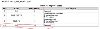
Register 0x173 = 0x0F
             PLL2_PRE_PD   0
                 PLL2_PD   0

Register 0x177 = 0x00
               PLL1R_RST   0

Register 0x182 = 0x00
        CLR_PLL1_LD_LOST   0
        CLR_PLL2_LD_LOST   0

Register 0x183 = 0x05
        RB_PLL1_DLD_LOST   0
             RB_PLL1_DLD   1
        RB_PLL2_DLD_LOST   0
             RB_PLL2_DLD   1

Register 0x184 = 0x50
       RB_DAC_VALUE[9:8]   1
           RB_CLKin2_SEL   0
           RB_CLKin1_SEL   1
           RB_CLKin0_SEL   0
           RB_CLKin2_LOS   0
           RB_CLKin1_LOS   0
           RB_CLKin0_LOS   0

Register 0x185 = 0xAF
       RB_DAC_VALUE[7:0]   2

Register 0x188 = 0x41
             RB_HOLDOVER   0
             RB_DAC_RAIL   0
             RB_DAC_HIGH   0
              RB_DAC_LOW   0
           RB_DAC_LOCKED   1

  • Hello Daniel,

    In your register map it seems you have the outputs (CLKout3, CLKout9, CLKout13) configured properly. On the other hand, I see that you have SYNC_1SHOT_EN=1, which I think may be the root of your problem. In the LMK0482x, the one-shot was duplicated separately for each SDCLKoutY path. In the LMK04832, the one-shot is now common to all outputs, and sits at the root of the SYSREF distribution path just after the SYSREF_MUX. Try again with SYNC_1SHOT_EN=0 and see if this works.

    Regards,

  • Hi Derek,

    Thanks for the feedback! The results after changing SYNC_1SHOT_EN to 0 are a bit odd. CLKout13 started working as expected (it outputs 2.5 MHz if I set SYSREF_MUX to continuous SYSREF), but CLKout3 and CLKout9 remain silent. I can't see any significant difference in configuration between the outputs in my register map. Especially not between CLKout13 and CLKout9 which have identical output configuration registers (0x120-0x127 and 0x130-0x137).

    After experimenting a bit, I tried changing the SCLKX_Y_DDLY setting from 8 to 0 (its POR default value). In LMK04826 a value of 0 meant bypass, not sure if it's the same for LMK04832, the register map doesn't state it explicitly. After this change, some signal appeared on CLKout3 and 9 as well. The signal has 2.5 MHz periodicity, and the half period where the output is low looks okay, but the half period where the output is supposed to be high looks odd. Either it's not driving the output properly during this half-period, or it's toggling too fast for my oscilloscope to measure accurately. CLKout13 still behaves differently and looks normal throughout the whole period. Does this have something to do with SYNC being level sensitive after the SYNC_1SHOT_EN change? Is it constantly resetting something during the high half-period? All the SYNC_DIS bits are set in register 0x144.

    Any idea why the outputs would differ in this way? And what the DDLY 0 / 8 behavior means?

    Regards,

    Daniel

  • Some additional testing: I tried changing all of the outputs of the PLL to output SYSREF in continuous SYSREF mode (both DCLKs and SCLKs). I set the output format to CMOS for any outputs that were not routed on the PCB so that they could still be measured on the pins of the chip. Measurement of the outputs showed the following:

    CLKout0 OK
    CLKout1 OK
    CLKout2 Bad
    CLKout3 Bad
    CLKout4 Bad
    CLKout5 Bad
    CLKout6 Bad
    CLKout7 Bad
    CLKout8 Bad
    CLKout9 Bad
    CLKout10 Bad
    CLKout11 Bad
    CLKout12 OK
    CLKout13 OK

    I then switched all outputs to output device clock instead, and modified all the channel dividers to get the same device clock frequency as I had when outputting SYSREF. In this configuration, all clock outputs showed normal output signal.

    The only pattern I can see is that the working outputs 0,1,12,13 all belong to clock group / Vcc group 0. The only clock group-specific thing I can find in the datasheet are the supply voltage pins per clock group. I've measured that all of these have 3.3V supplied. There's also the CLKoutX_Y_PD bits that have "power down entire clock group" in their description in the register map, but as far as I can tell those do not control clock groups but rather clock output pairs. Also, all these PD bits are zeroed during this test.

  • Hello Daniel,

    I tried changing the SCLKX_Y_DDLY setting from 8 to 0 (its POR default value). In LMK04826 a value of 0 meant bypass, not sure if it's the same for LMK04832, the register map doesn't state it explicitly.

    LMK04832 SCLKX_Y_DDLY is as LMK0482x sysref digital delay register.  The TICS Pro profile for LMK04832 reflects this properly with 0 = bypass.  I've put a note in for correction of the LMK04832 register map.  It appears LMK04832 is using a description from SYSREF_DDLY.

    The only pattern I can see is that the working outputs 0,1,12,13 all belong to clock group / Vcc group 0. The only clock group-specific thing I can find in the datasheet are the supply voltage pins per clock group. I've measured that all of these have 3.3V supplied. There's also the CLKoutX_Y_PD bits that have "power down entire clock group" in their description in the register map, but as far as I can tell those do not control clock groups but rather clock output pairs. Also, all these PD bits are zeroed during this test.

    Have you tried this test on more than one board?  Is there any possibility of solder down issue?  You mentioned confirming the 3.3 V is supplied.  Did you check by probing the pad / trace that the 3.3 V was supplied to the device with or by actually probing the small bit of the exposed pin of the LMK04832?

    When you set the bypass mode, this skips the SYSREF digital delay which is held in reset by SYSREF_CLR = 1.  You mention that SYSREF_CLR = 0.  But it does suggest that this block is preventing the signal from getting through, except that even when it is output, it's signal quality is different from the working output.

    Was the LMK04832 placed as a rework to a prior LMK04826?

    73,
    Timothy

  • Hi Timothy,

    Have you tried this test on more than one board?

    We sent a second board to be mounted with LMK04832 yesterday and I tested it just now. It shows identical behavior, same list of working / non-working output numbers and same type of output waveform issues when the SCLK digital delays are bypassed. It feels like this points to a systematic issue with how we configure the device, rather than a hardware error. Either that or the IC is incompatible with our PCB design somehow, but that would be odd as the LMK04826 works fine and they are supposed to be pin compatible. We're not using any CML outputs.

    Is there any possibility of solder down issue?  You mentioned confirming the 3.3 V is supplied.  Did you check by probing the pad / trace that the 3.3 V was supplied to the device with or by actually probing the small bit of the exposed pin of the LMK04832?

    We reviewed the soldering with a microscope when we noticed there were issues with SYSREF output and everything looked OK. The 3.3V supplies were probed on the exposed pin of the IC. 

    Was the LMK04832 placed as a rework to a prior LMK04826?

    Yes, both the boards previously had LMK04826 mounted (and were confirmed as functioning properly with LMK04826 prior to the rework).

    The register maps I included in my original post were all read out after finalized setup of the PLL. In case there's might be something wrong in terms of the order of our register writes or something like that, I've modified our SPI read/write code so that all reads and writes are dumped to a file and added some comments to the result.

    It doesn't look like I can attach files anymore in this new forum UI (?) but I've pasted it below:

    // Soft reset
    Write 0x000 = 0x80

    // Disable 3-wire
    Write 0x000 = 0x10

    // Write register map
    Write 0x002 = 0x00
    Write 0x15F = 0x3B
    Write 0x100 = 0xE8
    Write 0x101 = 0x08
    Write 0x102 = 0x03
    Write 0x103 = 0x60
    Write 0x104 = 0x20
    Write 0x105 = 0x00
    Write 0x106 = 0x00
    Write 0x107 = 0xF1
    Write 0x108 = 0xE8
    Write 0x109 = 0x08
    Write 0x10A = 0x03
    Write 0x10B = 0x60
    Write 0x10C = 0x20
    Write 0x10D = 0x00
    Write 0x10E = 0x00
    Write 0x10F = 0x11
    Write 0x110 = 0xE8
    Write 0x111 = 0x08
    Write 0x112 = 0x03
    Write 0x113 = 0x60
    Write 0x114 = 0x20
    Write 0x115 = 0x00
    Write 0x116 = 0x00
    Write 0x117 = 0x11
    Write 0x118 = 0xE8
    Write 0x119 = 0x08
    Write 0x11A = 0x03
    Write 0x11B = 0x60
    Write 0x11C = 0x20
    Write 0x11D = 0x00
    Write 0x11E = 0x00
    Write 0x11F = 0xF1
    Write 0x120 = 0xE8
    Write 0x121 = 0x08
    Write 0x122 = 0x03
    Write 0x123 = 0x60
    Write 0x124 = 0x20
    Write 0x125 = 0x00
    Write 0x126 = 0x00
    Write 0x127 = 0x44
    Write 0x128 = 0xE8
    Write 0x129 = 0x08
    Write 0x12A = 0x03
    Write 0x12B = 0x60
    Write 0x12C = 0x20
    Write 0x12D = 0x00
    Write 0x12E = 0x00
    Write 0x12F = 0xFF
    Write 0x130 = 0xE8
    Write 0x131 = 0x08
    Write 0x132 = 0x03
    Write 0x133 = 0x60
    Write 0x134 = 0x20
    Write 0x135 = 0x00
    Write 0x136 = 0x00
    Write 0x137 = 0x44
    Write 0x138 = 0x18
    Write 0x139 = 0x02
    Write 0x13A = 0x03
    Write 0x13B = 0xE8
    Write 0x13E = 0x00
    Write 0x13F = 0x0D
    Write 0x140 = 0x00
    Write 0x141 = 0x00
    Write 0x142 = 0x00
    Write 0x143 = 0x92
    Write 0x144 = 0x00
    Write 0x145 = 0x00
    Write 0x146 = 0x00
    Write 0x147 = 0x1A
    Write 0x148 = 0x0B
    Write 0x149 = 0x0B
    Write 0x14A = 0x02
    Write 0x14B = 0x16
    Write 0x150 = 0x01
    Write 0x151 = 0x02
    Write 0x152 = 0x00
    Write 0x153 = 0x00
    Write 0x154 = 0x04
    Write 0x155 = 0x00
    Write 0x156 = 0x04
    Write 0x157 = 0x00
    Write 0x158 = 0x96
    Write 0x159 = 0x00
    Write 0x15A = 0x01
    Write 0x15B = 0x14
    Write 0x15C = 0x3F
    Write 0x15D = 0xFF
    Write 0x160 = 0x00
    Write 0x161 = 0x01
    Write 0x162 = 0xA4
    Write 0x163 = 0x00
    Write 0x164 = 0x00
    Write 0x165 = 0x05
    Write 0x173 = 0x0F
    Write 0x166 = 0x00
    Write 0x167 = 0x00
    Write 0x168 = 0x05
    Write 0x169 = 0x59
    Write 0x16A = 0x3F
    Write 0x16B = 0xFF
    Write 0x16C = 0x00
    Write 0x16D = 0x00
    Write 0x173 = 0x0F

    // 500ms sleep, then wait for PLL1 + PLL2 lock
    Read 0x183 = 0x0F
    Read 0x183 = 0x0F

    // Set SYSREF_MUX to SYNC pin, SYNC mode to SYNC pin
    Read 0x139 = 0x02
    Write 0x139 = 0x00
    Read 0x143 = 0x92
    Write 0x143 = 0x91

    // Clear all SYNC_DIS bits
    Write 0x144 = 0x00

    // Toggle SYNC_POL
    Read 0x143 = 0x91
    Write 0x143 = 0xB1
    Write 0x143 = 0x91

    // Set all SYNC_DIS bits
    Write 0x144 = 0xFF

    // Clear SYSREF_CLR bit
    Read 0x143 = 0x91
    Write 0x143 = 0x11

    // Set SYSREF_MUX to SYSREF continuous, set SYNC mode to prevent SYNC events
    Read 0x139 = 0x00
    Write 0x139 = 0x03
    Read 0x143 = 0x11
    Write 0x143 = 0x10

    // Clear LD_LOST for both PLLs
    Write 0x182 = 0x03
    Write 0x182 = 0x00

    // After this I measure the outputs (which are all set to output continuous SYSREF,
    // and only outputs 0-1 and 12-13 look correct, the rest have half-corrupt waveforms)

    Best regards,

    Daniel

  • I captured some images from the oscilloscope of the working/non-working outputs in case that helps. All of these were taken with the PLL in the same state, no reconfiguration in between.

    Here's the P/N pins of CLKout12, an LVPECL output, which looks OK:

    Here's CLKout8, also an LVPECL output, but one of the outputs that gives a corrupt waveform. It looks stable during the half period when the output is logic low, and floats to a noisy middle voltage during the other half period.

    I'm using a 1GHz scope with passive probes, so the noisy stuff could also be something that's above the frequency range I can capture.

    Here's CLKout0, an LVDS output (although it's currently unterminated on the board). Looks OK:

    And here's CLKout3, also an LVDS output, but with bad output:

    For CLKout3 it's not as obvious that anything is changing at all (compared to CLKout8), but here's a plot of the + output with the scope set to AC-coupled and zoomed in a lot, which shows that the output is moving around at 2.5 MHz although only by a few tens of millivolts:

    And note that both CLKout3 and CLKout8 start looking like the working outputs if I switch them to output device clock instead of SYSREF.

    I probed some of the non-working outputs that are set to CMOS as well, but they look like they remain at 0V out without any discernible movement.

  • Hello Daniel,

    The LMK04832 is pin compatible with LMK04826.  However it is not 100% programming compatible.  The most differences are in the output buffer... while I did import this and it the config seemed reasonable... I'm going to look closer Monday.  I'll confirm with an EVM too.

    In the meantime can you confirm...

    CLKin0/1 = 10 MHz  (I note you don't have CLKin0/CLKin1 enabled).
    VCXO = 100 MHz
    VCO = 2500 MHz
    OUT2 = 312.5 MHz
    OUT3 = 2.5 MHz from SYSREF.

    73,
    Timothy

  • Hi Timothy,

    The LMK04832 is pin compatible with LMK04826.  However it is not 100% programming compatible.

    Yes, I've been testing with a modified programming sequence to fit the LMK04832 register map, not the same programming sequence that we used for LMK04826. 

    I'm going to look closer Monday.  I'll confirm with an EVM too.

    That would be great!

    In the meantime can you confirm...

    CLKin0/1 = 10 MHz  (I note you don't have CLKin0/CLKin1 enabled).
    VCXO = 100 MHz
    VCO = 2500 MHz

    I can confirm these. I'm using CLKin1, by selecting it via CLKin_SEL_MANUAL. The CLKin auto-selection and selection via CLKin_SEL pins features have been disabled, which should mean that the CLKin_SEL_MANUAL setting overrides the EN_CLKin bits according to the datasheet.

    OUT2 = 312.5 MHz
    OUT3 = 2.5 MHz from SYSREF.

    These are correct for the register values in my original post. OUT9 and OUT13 are also 2.5 MHz from SYSREF.

    If you use the original post register dump, maybe make sure to set SYNC_1SHOT_EN to 0 as well as per Derek's recommendation, and also all the SCLKX_Y_DDLY registers (0x106, 0x10E, etc) to 0 as doing that was what allowed me to see the corrupt output waveforms, otherwise the outputs were silent.

    In my later posts, I was attempting to troubleshoot the SYSREF issues, so in the register write/read sequence I posted recently, all the outputs OUT0-OUT13 are 2.5 MHz from SYSREF. 

    Best regards,
    Daniel

  • Sorry Daniel,

    I'm a little delayed.  I'll post again.

    73,
    Timothy

  • Hello Daniel,

    I reviewed and found the root cause to be programming 0x173 = 0x0F.  It should be 0x10.  This register has some reserved bits which should be set to 0x10.

    Having said that I also found several registers being programmed that are not in the LMK04832 register map.  I have not programmed these, the TICS Pro software will throw out these invalid register programmings.

    I've updated a raw_register_map which sets 0x17310, includes the 1_SHOT update, and also removes registers not in the register map.  Also, as per the recommendation for programming sequence, I simply moved the 0x166, 0x167, 0x168 register programming to the end to ensure all necessary registers were programmed before starting PLL2 calibration.  Loading this should give you the operation you expect.

    0x00010
    0x00100
    0x00200
    0x00306
    0x00463
    0x005D1
    0x00C51
    0x00D04
    0x1000A
    0x10100
    0x10200
    0x10300
    0x10434
    0x10500
    0x10608
    0x10701
    0x10808
    0x10900
    0x10A00
    0x10B00
    0x10C20
    0x10D00
    0x10E08
    0x10F11
    0x11008
    0x11100
    0x11200
    0x11300
    0x11410
    0x11500
    0x11608
    0x11711
    0x118FA
    0x11900
    0x11A00
    0x11B00
    0x11C34
    0x11D00
    0x11E08
    0x11F01
    0x12001
    0x12100
    0x12260
    0x12300
    0x12420
    0x12500
    0x12608
    0x12744
    0x12808
    0x1290A
    0x12A80
    0x12B50
    0x12C10
    0x12D00
    0x12E01
    0x12F00
    0x13001
    0x13100
    0x13260
    0x13300
    0x13420
    0x13500
    0x13608
    0x13744
    0x13818
    0x13903
    0x13A03
    0x13BE8
    0x13C00
    0x13D08
    0x13E00
    0x13F0D
    0x14000
    0x14180
    0x14200
    0x14310
    0x144FF
    0x14500
    0x14600
    0x1471A
    0x1480B
    0x1490B
    0x14A02
    0x14B16
    0x14C00
    0x14D00
    0x14E00
    0x14F7F
    0x15009
    0x15102
    0x15200
    0x15300
    0x15404
    0x15500
    0x15604
    0x15700
    0x15896
    0x15900
    0x15A01
    0x15B14
    0x15C3F
    0x15DFF
    0x15E1E
    0x15F3B
    0x16000
    0x16101
    0x162A4
    0x16300
    0x16400
    0x16505
    0x16959
    0x16A3F
    0x16BFF
    0x16C00
    0x16D00
    0x16E06
    0x17310
    0x17700
    0x18200
    0x18305
    0x18450
    0x185AF
    0x18841
    0x16600
    0x16700
    0x16805
    

    73,
    Timothy

  • I reviewed and found the root cause to be programming 0x173 = 0x0F.  It should be 0x10.  This register has some reserved bits which should be set to 0x10.

    Thanks Timothy, looks like this is the issue, changing this value fixed the outputs. I must have misread the default value as 15 instead of 16.

    Having said that I also found several registers being programmed that are not in the LMK04832 register map. 

    In the register dump I just read out every register between 0x100 and 0x188 from the IC. We're not actively writing values to all the registers listed, so this should be OK.

    Thank you for the help!

  • Glad all is working for you.

    73,
    Timothy