This thread has been locked.

If you have a related question, please click the "Ask a related question" button in the top right corner. The newly created question will be automatically linked to this question.

LMK03806: USB2ANY - LMK03806 connection Uwire

Part Number: LMK03806
Other Parts Discussed in Thread: USB2ANY, LMX2581

Hello,

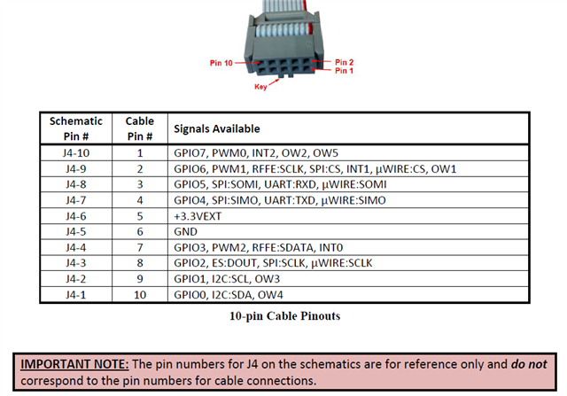
I would like to know how to connect to LMK03806 by USB2ANY 10-Pin Cable (J4)

I use USB2ANY Interface Adapter (ti.com) (page 14) for the reference

Pin2: µWIRE:CS

Pin3: µWIRE:SOMI

Pin4. µWIRE:SIMO

Pin8. µWIRE:SCLK

But in page 12 we also have :((

Pin3: SCLK

Pin7.SIMO

Pin8: SOMI

Pin9: CS

Someone can explain pls!

Merci

  • Hello,

    Unfortunately the USB2ANY has a cable polarity backwards, therefore the pins are flipped.  Please note the schematic pin number vs cable pin number on table 2 on page 14.

    73,
    Timothy

  • Thank you Timothy for your answer,

    Do I need an Adapter Board to connect USB2ANY to LMK03806 or I connect them directly by using Uwire?

    Thank you. 

  • So you can't directly connect the USB2ANY to the LMK03806.  However you can simply use jumpers to interface the two boards.  Can you advise, when you got your EVM, what did it include for cables?

  • I am sorry because my question was not clear.

    In fact, I did not buy LMK03806 EVM, but we have a board is designed by my colleague in which we use LMK03806.

    So we used the cable and USB2ANY which is included in EVM LMX2581 EVM (We bought it in a previous project)

    The direct connection means I connect 2 boards using jumpers (the cable 10 pins  <--> the PMOD jumper in my boards)

    I saw that we can program EVM LMX2581 EVM directly using the 10 pins cable without any Adapter Board, but with our board, it can not. 

    Do you have any ideas?

  • I have to see the schematic of your board.  It should be possible.  But my guess is you were probably tricked by the flipped pin-out of the USB2ANY and need to rotate your cable 180 degrees.

    Are you able to probe for the clock, data, and LE on the board you designed to see where the USB2ANY is "delivering" it?

    73,
    Timothy

  • I've also checked very carefully the pin maps of the two connectors.

    I can verify that we received a good signal of SPI-Uwire at the connector PMOD on the board at the pin that we want.

    However, we could not see any signal at the 14 outputs clock of LMK03806. 

    I think we need to debug the board before posting it here maybe someday for sure. ;)

  • This is the capture of signal SPI-uwrie at the connector in my board

  • Hello Van-dung PHAM,

    Those look like some really nice signals I presume the correct signal is on the correct pin.  For example clock on clock, etc.

    At start up without any program you should see a clock at CLKout8 and OSCout0.  OSCout0 should be a buffered copy of the OSCin and CLKout8 should be nominally 98 MHz.

    If you don't see those clocks, then there's probably something very fundamental wrong.

    73,
    Timothy

  • sorry for my late reply,

    You are right

    I set up the 10 MHz configuration on TICS Pro and I saw only one output at OSCout0 which is 10 MHz (We used a 10MHz OCXO Oscillator) but I did not see the output at CLKout8.

    Are there any important parameters that can change the game?

    Thank you

  • Hello Van-dung PHAM,

    You mentioned setting up the configuration on TICS Pro, are you able to turn off OSCout by powering it down through programming?

    If you are just powering the device up, then see the 10 MHz from OSCout - but no output from CLKout8.
      - Check the SYNC pin input state.  As I recall it should be low.
      - Please confirm 3.3 V on each supply pin.

    73,
    Timothy

  • Thank you

    I am sorry but I can not turn off OSCout by powering it down through programming in TICS PRO.

    3.3 V on each supply pin is confirmed.

    In terms of SYNS? In your answer above, there are just only 4 pins: 

    Pin2: µWIRE:CS

    Pin3: µWIRE:SOMI

    Pin4. µWIRE:SIMO

    Pin8. µWIRE:SCLK

    So please tell me Pin SYNC come from where in 10-PIN IDC cable? and what is the correct connection?

    Best,

  • Mousing over SYNC pin in the Pins group at the bottom of the User Controls page shows that USB2ANY GPIO1 is the SYNC pin in the text window on the left hand side. 

    So that is cable pin #9.

    73,
    Timothy

  • Thank 

    I got this result from your help.

    It looks good for me in terms of VOD (≈400mV) and frequency (10 MHz)

    However, all of the clock outputs had not in the same phase.

    In my application, I would like to have all of the 14 outputs clocks have the same phase and frequency.

    Maybe I skip one of the important parameters in TICS PRO?

    R0 (INIT)	0x00020200
    R0	0x00001F40
    R1	0x00001F41
    R2	0x00001F42
    R3	0x00001F43
    R4	0x00001F44
    R5	0x00001F45
    R6	0x11110006
    R7	0x11110007
    R8	0x11110008
    R9	0x55555549
    R10	0x1142400A
    R11	0x3401100B
    R12	0x130C006C
    R13	0x3B03826D
    R14	0x0300000E
    R16	0xC1550410
    R24	0x00000018
    R26	0xAFA8001A
    R28	0x0010001C
    R29	0x0080033D
    R30	0x0500033E
    R31	0x001F001F

    I am sorry if I posed a stupid question because I am a newbie in this domain.

    Best,

  • Hello Van-dung PHAM,

    No problem.  To sync all the outputs, you will need to either provide software programming to perform sync by toggling the sync polarity or toggling the SYNC pin.

    Does that solve your issue?

    73,
    Timothy

  • Hello Timothy

    Do you mean this option in TICS Pro? I already toggled it.

    I would like to attach the TCS file for more detail.

    Thank you

  • THis is the TCS file

    [SETUP]
    ADDRESS=888
    CLOCK=8
    DATA=4
    LE=2
    PART=LMK03806B
    IFACE=UWIRE
    ADDRESS_I2C=0x0
    
    [PINS]
    PINNAME00=SYNC
    LOCATION00=1
    PINVALUE00=True
    PINNAME01=TRIGGER
    LOCATION01=10
    PINVALUE01=True
    
    [MODES]
    NAME00=R0 (INIT)
    VALUE00=131584
    NAME01=R0
    VALUE01=8000
    NAME02=R1
    VALUE02=8001
    NAME03=R2
    VALUE03=8002
    NAME04=R3
    VALUE04=8003
    NAME05=R4
    VALUE05=8004
    NAME06=R5
    VALUE06=8005
    NAME07=R6
    VALUE07=286326790
    NAME08=R7
    VALUE08=286326791
    NAME09=R8
    VALUE09=286326792
    NAME10=R9
    VALUE10=1431655753
    NAME11=R10
    VALUE11=2495758346
    NAME12=R11
    VALUE12=872484875
    NAME13=R12
    VALUE13=319553644
    NAME14=R13
    VALUE14=990085741
    NAME15=R14
    VALUE15=50331662
    NAME16=R16
    VALUE16=3243574288
    NAME17=R24
    VALUE17=24
    NAME18=R26
    VALUE18=2947022874
    NAME19=R28
    VALUE19=1048604
    NAME20=R29
    VALUE20=8389437
    NAME21=R30
    VALUE21=83886910
    NAME22=R31
    VALUE22=2031647
    OSCIN00=10
    EXTRA_PLL_N_DIV_1_00=0
    
    [FLEX]
    CLKout0_FREQ=10
    CLKout10_FREQ=10
    CLKout11_FREQ=10
    CLKout1_FREQ=10
    CLKout2_FREQ=10
    CLKout3_FREQ=10
    CLKout4_FREQ=10
    CLKout5_FREQ=10
    CLKout6_FREQ=10
    CLKout7_FREQ=10
    CLKout8_FREQ=10
    CLKout9_FREQ=10
    OSCout0_FREQ=10
    OSCout1_FREQ=10
    PLL_PDF_FREQ=20
    PLL_REF_FREQ=10
    VCO_FREQ=2500
    bSync=SYNC
    stStatus=OSCin Frequency = 10.0 MHz
    

  • Even I've already performed sync by toggling the SYNC pin, but I did not get good results. There are just only 10 outputs that had the same frequency and the same phase. (From clk3 to clk11 )

    phase retardation of Clk0 and Clk1 is 154 degree

    phase retardation of Clk12 and Clk13 is 145 degree

    Is there any mistake in my configuration file? Slight smile

  • Hello Van-dung PHAM,

    Sounds like all your outputs are the same frequency, 10 MHz... just not the same phase?

    The problem here is that what you call CLKout12/13 are not actually clock outputs, but OSCout.  OSCout is a buffered copy of OSCin.  The timing after sync wouldn't align these to the CLKout0 to 11.  Also, there would be a increase in skew between these two groups of CLKout and OSCout since the path is different through the IC.

    So you are receiving the expected behavior.

    Is this problematic for you?  Or did you just need to confirm the device was working properly.

    73,
    Timothy

  • Thank you for your answer.

    Actually, in our design clk0 and clk1 are connected to 2 output single-end SMA (the others are differential output).

    That the reason why we have a different phase in clk0 and clk1

    For the clk12 and clk13, the reasons as you have explained. Slight smile

    Our design needs at least 12 outputs that have the same phase and frequency. Then I think we need to modify the design (just change clk12&13 to clk1&2)

    Best,

  • Hello Van-dung PHAM,

    Sounds like that will meet your objective.

    73,
    Timothy