This thread has been locked.

If you have a related question, please click the "Ask a related question" button in the top right corner. The newly created question will be automatically linked to this question.

SE555: Sequential Timer Circuit

Part Number: SE555

Hello,

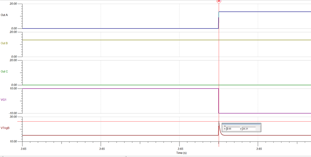
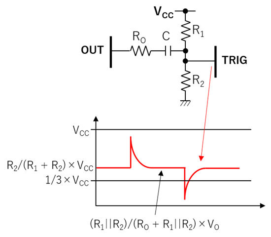
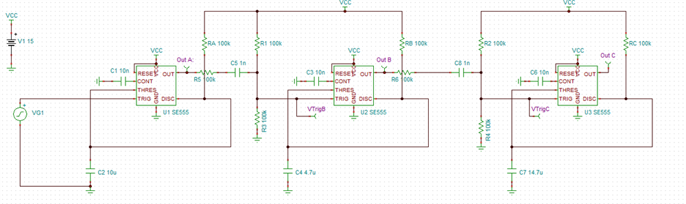
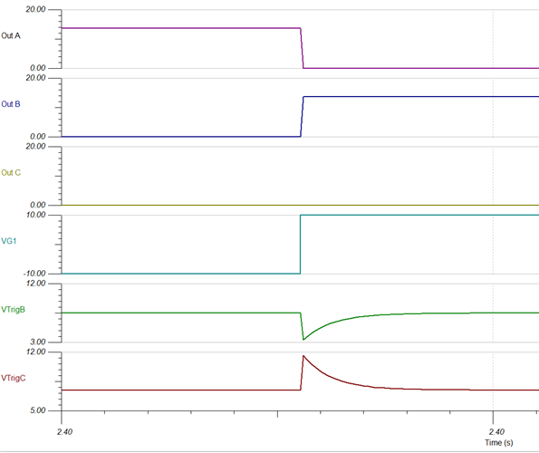
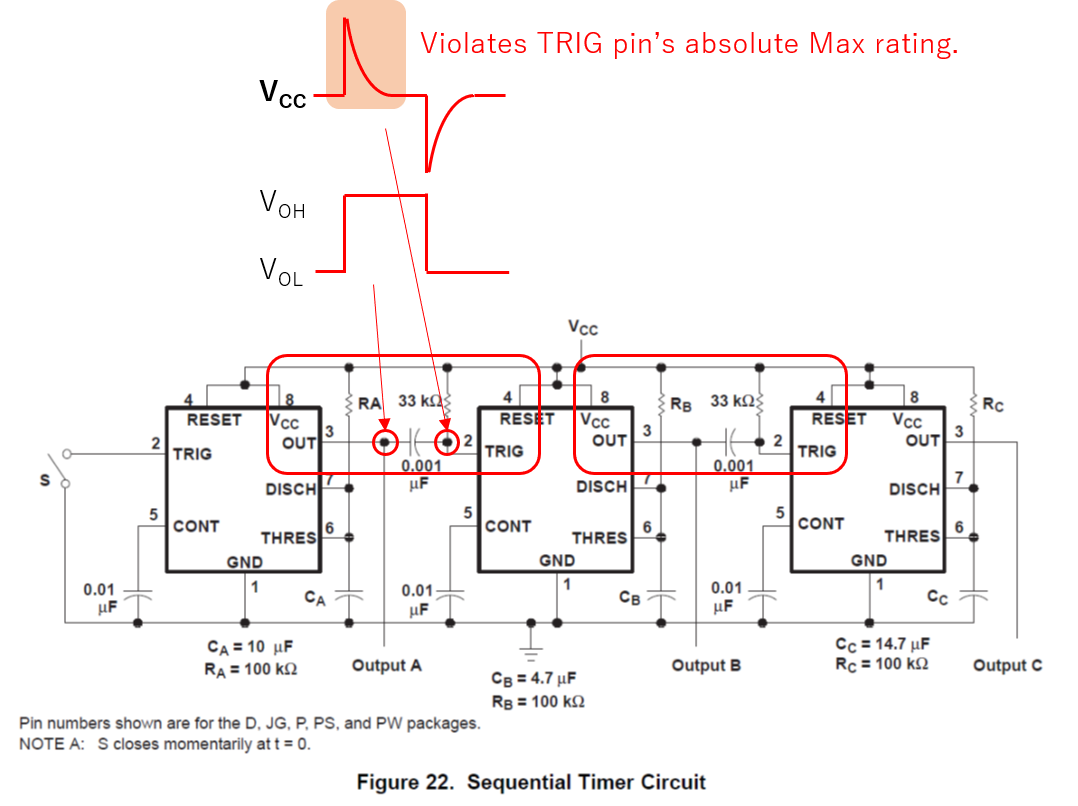
I've noticed SE555's sequential timer circuit in Figure 22 of its data sheet violates its TRIG pin's absolute Max rating. Do you agree with me? The TRIG pin's absolute Max rating is defined as VCC (Max), but the pin's waveform after an RC circuit exceeds the VCC when an OUT pin voltage of the previous stage rises.

Do you have any workaround for this?

Best regards,
Shinichi Yokota

  • Hello,

    Great catch! I see this in simulation as well. I have lowered the 0.001uF (1nF) down to 1pF in simulation and in addition formed a voltage divider to lower the dv/dt. I have attached the simulation for you as well at the bottom of the post. 

    For the 1nF case I am seeing the voltage spike up to 26.31V in simulation (Datasheet circuit). This appears to be due to C*dv/dt. By lowering these two factors I was able to smooth out the trigger lines as see in the second simulation below. 

    Datasheet Circuit

    My Revised Circuit with simulation below:

    SE555 Sequential Timer Circuit.TSC

  • Chris-san,

    Thanks for your feedback. However, I'm afraid to say I don't think a positive spike on the TRIG pin disappears. The time constant of the RC circuit is 50 ns (= 1 pF × (100 kΩ || 100 kΩ)), which is very small, and I guess it just doesn't show up in the simulation plot due to the large time scale (in a sec range). Besides, I think a 1-pF capacitor is not realistic for a real PCB as it's as small as parasitic capacitance on PCB.

    I've come up with the following circuit. I added a RO to the OUT pin of the previous SE555 stage to attenuate the VO amplitude so that its positive spike won't exceed the VCC. How do you think? I need to take into account variations of the component values, though, if the circuit goes into production.

    Best regards,
    Shinichi Yokota

  • Shinichi-san,

    Yes this looks very reasonable. I did the same on my side and this looks good. You are correct on the PCB parasitics playing a larger role with a smaller capacitor. I used this for demonstration purposes in order to see the reduction of C*dv/dt.

    Your solution looks great! I switched my components such that the capacitors are 1nF and I chose 100k for testing purposes. These of course are subject to change depending on the spikes seen in circuit. The larger the cap, the less susceptible it is to parasitics however, the larger the C*dv/dt the larger the spikes. Having these placeholders on your board for the R's and C will give you a lot of flexibility to adjust accordingly. 

  • Shinichi-san,

    You could also place a reverse bias diode from the trigger pin to the supply. That way if the voltage exceeds the supply the diode will absorb the pulse. A TVS diode may be considered. This can be in addition to our other considerations so you have flexibility in your design. At a minimum have the footprints available on your board so you don't have to re-spin it.