This thread has been locked.

If you have a related question, please click the "Ask a related question" button in the top right corner. The newly created question will be automatically linked to this question.

LMK04828: Multi-board LMK Sync

Part Number: LMK04828
Other Parts Discussed in Thread: LMK04832

Hi,

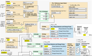
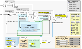
We want to use LMK04828 CLK synthesizer for RFSoC FPGA for multi-board synchronization (ADC/DAC sampling)

Below are the specs

1] ADC sampling rate = 1350Mhz

2] DAC sampling rate = 5400MHz

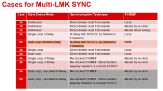
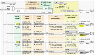
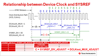
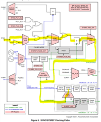
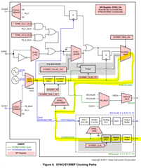
We are following "Synchronization Method: ZDM" with the below rules

So please verify my clock scheme for multi-board SYNC

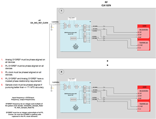
Keeping into rules in account

ADC/DAC CLK = 337.5MHz

SYSREF = 5.625MHz

I/P REF FREQ = 5.6225MHz


Please validate the same

  • Hello Shekhar,

    This approach looks generally good.  Here are a few comments.

    (1) If you use LMK04832, then your 160 MHz VCXO can run at 320 MHz phase detector frequency for PLL2 (160 MHz doubled) vs. 80 MHz on LMK04828 (max PDF of 155 MHz).  This would give you a performance boost.

    (2) You show Dout8 as 337.5 MHz and SDout3 as 5.625 MHz.  I would suggest using the even-odd pairs for your device clocks & SYSREF.  So for example Either Dout8 = 337.5 MHz and SDout9 = 5.625 MHz or Dout2 = 337.5 MHz and SDout3 = 5.625.

    (3) This is the biggest detail in your implementation.  In relationship to your specified condition #1 and #2 (In which case you will have #4 also).  Are you planning on using pulsed SYSREF or continuous SYSREF?  (3a) If you use continuous SYSREF, then the SYSREF phase will be aligned.  We don't recommend running continuous at all times because of crosstalk concerns and you could save power if you turn them off.  However it is a valid technique to run continuous for a short amount of time, synchronize the JESD204B receivers - typically by...
      - Turning on continuous SYSREF
      - Waiting for AC coupled SYSREF to stabilize
      - Telling the JESD204B receivers to stop listening to SYSREF, while meeting a setup and hold time to the SYSREF frequency for all receivers.
      - Then off continuous SYSREF.

    (3b) If you use pulsed SYSREF, then the physical interface from LMK04828 to receiver is best to be DC coupled and you must request SYSREF from both LMK04828 devices at the same moment to cause the SYSREF output to be aligned.  Otherwise they may be off in time by n*SYSREF period.  (Which is acceptable for general JESD204B synchornization).  There are a few ways to generate the SYSREF pulse:
      (i) Use SYSREF pulser mode and request SYSREF pulse by software meeting a setup and hold time to PLL1 reference.
      (ii) Use SYSREF pulser mode and request SYSREF pulse by SYNC pin meeting a setup and hold time to PLL1 reference.
      (iii) Use SYSREF re-clocked mode (SYSREF_MUX selects D flip-flop input), and provide a SYSREF/SYNC input on SYNC pin meeting a setup and hold time to the PLL1 reference.
      (iv) Use SYSREF re-clocked mode (SYSREF_MUX selects D flip-flop input), and provide a SYSREF/SYNC input on CLKin0 meeting a setup and hold time to the PLL1 reference.

    Note, from the JESD204B spec, it does not require to have SYSREF at the same moment in time to your JESD204B recevier.  Only that the time modulus the LMFC clock period is the same.  Which means you don't need to worry about any setup and hold time.  The LMK04828 will take care of providing the SYSREF no matter when you request it.
       - My interpretation of your design conditions suggest you do expect this alignment and therefore must take into account the setup and time.

    (4) You need to decide which clock input to use for your 5.625 MHz input.  I suggest leaving CLKin0 availible do you can have the option to use it for SYSREF/SYNC related input functions.  In general, I suggest connect your 5.625 MHz input to CLKin1 or CLKin2, not CLKin0.

    --

    Here are two suggestions which may work for you to generate a SYSREF pulse at the same moment from both devices.

    The simplest solution is to have an LMK04832 generate the 5.625 MHz reference (LMK04832 has big dividers on each device clock output) to CLKin1 of each device, then provide a 5.625 MHz SYSREF signal which goes to CLKin0 of each device.  This is method 3b,iv above.  On the LMK04832 you can adjust the timing on the SYSREF to each LMK04828 (or LMK04832) which will then re-clock the SYSREF on to the JESD204B target.
      - Then use the SYSREF pulser feature on LMK04832 to launch the SYSREF pulses to downstream devices.

    The second option is to have one of your LMK04828 produce a SYSREF output to the next board or for N many other boards.  Connect this sysref output to CLKin0, the timing can be adjusted relative to the 5.625 MHz reference.
      - Then use the SYSREF pulser feature on the upstream LMK04828 to launch the SYSREF pulses to it's own JESD204B targets and to the downstream LMK04828 which will re-clock and output the SYSREF.  The trouble with this is the pipleline delay may be to great to give you a lot of flexibility in placement of the SYSREF to ensure all JESD204B receive the SYSREF at the exact same moment.  However it would be deterministic.  With LMK0482x (vs LMK04832) it is possible to reduce pipeline delay by using the SYSREF_CLKin0_MUX to bypass the CLKin0 based some of the initial circuitry.  Both LMK0482x and LMK04832 do allow you to bypass the SYSREF digital delay also.  With LMK0482x I've seen it possible to two devices together and have SYSREF output at the same time.  At least for some conditions.


    73,
    Timothy

  • Hi Timothy,

    Thanks for the reply, I shall consider even-odd pairs for your device clocks & SYSREF.

    we are following the below methodology for multi-LMK sync (2b), Ref Freq = Sysref Freq

    Also Synchronization method as Zero Delay Mode, wherein ZDM rule is met, I do not need pulsed SYSREF to occur at the same time for both devices, using Dual loop mode with low Freq to PLL1

    After the above considerations, will my scheme is fine?

    NOTE: I do not want to use any Master/root LMK, neither I have a plan/scheme/option of using SYNC/CLKIN0 for sync purposes. 

  • Hello Shekhar,

    As you mention - if SYSREF doesn't have to occur at the same moment on multiple boards, then it is easy and your scheme is fine.  I agree no need for a root LMK.

    73,
    Timothy

  • Hi Timothy,

    Modified Requirement

    1] DCLK = 112.5MHz (Use internal RFSoC PLL to get 1350MHz)

    2] SDCLK = 5.625MHz (Integer multiple of sampling CLK/16 i.e. 1350/16 = 84.375)

    Now for this, we are using the below settings in TICS Pro

    1. Input CLKIN0 is configured as 5.625MHz
    2. The PLL1 phase detector is also configured as 5.625MHz
    3. External VCO is chosen as 225MHz
    4. The internal VCXO should be in the range of (2370 - 2630)MHz or (2920 - 3080MHz)MHz
    5. The VCXO mux is configured as VCO0 as the frequency which has chosen is 2475MHz, 2475MHz is chosen because 2475/440 gives us 5.625MHz as the sys ref frequency
    6. The feedback path is chosen as FB_MUX which eventually is SYSREF (Nested 0 Delay F/B)

    1. SYSREF clock divider is chosen as 440 to get SYSREF Frequency as 5.625MHz
    2. SYSREF_MUX is chosen as SYSREF continuous
    3. SYSREF_CLKin0_mux is chosen as from SYSREF_MUX
    4. From this configuration, we get the SYSREF_Frequency

    1. DCLKs are used to generate high frequency, and SDCLK are used to generate low frequency
    2. DCLK frequencies can be generated only through Internal VCXO Divider and SDCLK frequencies can be generated as SYSREF Frequency
    3. As the SYS_REF we require is the same as the SYS_REF generated, it doesn't need to pass through any dividers, the clock output selection can be made SYSREF as shown. 
    4. Clock divider value is chosen as 22 to get 112.5MHz

    Please Validate the scheme and suggest changes if any...

    Thanks 

    Shekhar

  • Hello Shekhar,

    Were/are you able to test this on your board and system to determine if it meets your requirements?  At the end of the day you'll need to confirm everything as you need performance wise, etc.  For example, any possible spurs because of running SYSREF in continuous mode.  Observe there is no separation between DCLKoutX and SDCLKoutY.

    External VCO is chosen as 225MHz

    I think you mean external VCXO frequency is chosen as 225 MHz.  It's ok if really it is an external VCO so long as you are satisfied with the performance.

    The internal VCXO should be in the range of (2370 - 2630)MHz or (2920 - 3080MHz)MHz

    Internally we have VCOs.

    DCLK frequencies can be generated only through Internal VCXO Divider and SDCLK frequencies can be generated as SYSREF Frequency

    There is no internal VCXO divider.  Perhaps you are referring to the channel dividers from the VCO?  Both the device clock and SYSREF are generated from the dividers from VCO in this configuration.  This is ok.

    As the SYS_REF we require is the same as the SYS_REF generated, it doesn't need to pass through any dividers, the clock output selection can be made SYSREF as shown. 

    Everything appears selected properly.  However the SYSREF is produced by the SYSREF divider from the VCO.

    73,
    Timothy

  • Hi Timothy,

    We are planning to carry out the expt in Xilinx RFSoC EVAL board (This has an LMK module)

    Also, tell us to go ahead with LMK04828 orLMK04832.

    And can we go ahead with the above set Phase Detector freq for both PLL1 and PLL2

  • Also, tell us to go ahead with LMK04828 orLMK04832.

    In general, so long as you don't need CLKin0 --> CLKout, or need SYSREF at the same moment using two cascaded devices -- I suggest the LMK04832.

    And can we go ahead with the above set Phase Detector freq for both PLL1 and PLL2

    The LMK04832 will allow you to run PLL2 at 320 MHz.  PLL1 will still need to be the lower 5.625 MHz (or lower).  But this is of no concern because the VCXO will do jitter cleaning.

    73,
    Timothy

  • Hi Timothy,

    In one of the similar projects, we need our output clocks to be in phase with each other but not to be in phase w.r.t. input ref clock.

    So can we ignore the first rule of ZDM i.e. I/P CLK = GCD (O/P CLK, I/P CLK), and only follow the 2nd rule i.e. lowest o/p freq as SYSREF feedback in ZDM nested topology?

    With this, we shall get Deterministic phase w.r.t I/P. 

  • Hi Shekhar,

    Since Timothy is OoO I can answer. Consider the case where the input ref clock is twice the frequency of the SYSREF, for simplicity. There are two possible phases for each LMK input phase detector due to the R-divide, and since the SYSREF is aligning to this phase detector, it is possible for there to be two SYSREF phases as well. Even if you reset the SYSREF divider phase, without knowing the R-divider phase on every device, there is no way to guarantee the output phase on every device will be the same.

    Actually, LMK04832 has the capability to reset the R-dividers (LMK0482x do not). So it is technically possible to set the R-divider phase manually on every device, allowing LMK04832 to ignore the first rule of ZDM. To synchronize every device, first all R-dividers would be simultaneously reset. Then a SYNC event could be generated, and as long as the SYNC event is quick (a few ns) such that there is no possibility for cycle slip after the dividers begin dividing again, every output would be in phase and there would only be one possible phase for every output. This would be true only for cases where the input clock is a multiple of the SYSREF, as there is no way to reset the N-divider specifically.

    If the SYSREF frequency is not the phase detector frequency (i.e. if the N-divider to the input phase detector is not 1), it is no longer possible to use any ZDM rules to your advantage in input-to-output synchronization. In this case, you must synchronize the output dividers manually, within the same VCO cycle on each device - inevitably a CLKin0 SYNC, dynamic digital delay, or some other mechanism for compensation would be required.

    Regards,

    Derek Payne

  • Hi Derek,

    Thank you for the explanation.

    Actually, I forgot to mention that the other similar project which I mentioned above has only 1 single LMK04828. 

    In this case, I need at any power on time, my O/P's of LMK to be in phase and not be with the I/P ref clock.  

    (Because, as u mentioned SYSREF can take any phase, but as I have a single device, I can be assured that SYSREF can be in one of the phases at one single time)

    If my System/Project has multiple LMKs, then all the ZDM rules must & should be taken care of.  

    Please correct me, If I am wrong. 

  • Shekhar,

    Thanks for the clarification. I agree with your statements. If all you have is a single device, and the input to output phase relationship is inconsequential, you can just program the delays and SYNC the dividers without worrying about timing constraints; the SYNC will establish the phase relationship between all output dividers (including the SYSREF divider).

    Regards,

    Derek Payne

  • Hi Derek,

    For the above design, I won't be using any Sync, I will just use SYSREF DIV as F/B to PLL1 in ZDM but my I/P ref clock (CLKIN0) is independent of SYREF.

    i.e. Only 2nd rule of ZDM is followed

    Please correct me.  

  • Hi Shekhar,

    When you program the device, the divider state is effectively random. Nothing about the zero-delay rules will guarantee phase alignment between any of the device clocks and SYSREF on the same device - it just guarantees a relationship between the SYSREFs running on multiple devices with the same input clock phase. The big benefit of using the ZDM config with the SYSREF in the feedback path is that the SYSREF can also re-time SYNC pulses to a precise VCO clock cycle, without any complicated timing for the user. This SYNC could even be generated entirely in software, by toggling the SYNC_POL bit, or by triggering the SYNC off of lock detect using SYNC_PLLx_DLD bits. But one way or another, the output dividers need to have their phase relationship established with a phase sync, no matter what. This is also true for the multi-device scheme.

    The benefit of following the ZDM rules in the multi-device scheme is:

    • Since GCD(outputs, inputs) = input, there is only one possible isochronous phase for every PLL's phase detector
    • Since the SYSREF divider is in the feedback path, there is only one possible phase for every SYSREF in the system
    • Since GCD(outputs) = SYSREF, all device clocks can share an edge with the SYSREF edge (or be delayed an arbitrary amount from the SYSREF edge)
    • Since the SYSREF can re-time SYNC events, every device can re-time an asynchronous SYNC pulse to align all device clock dividers to the SYSREF divider, and therefore to each other, across all devices

    If you only have one device, and that device doesn't need to have a reproducible input-to-output phase relationship, there isn't really a reason you would have to follow the ZDM rules for reproducible phase relationships. You could just introduce an arbitrarily-timed software SYNC and set the device clocks/SYSREF phase relationship that way. The key benefit of the ZDM rules is that they establish a guaranteed way to produce an isochronous SYNC event on multiple device by meeting setup/hold time to a SYSREF clock running in the low MHz range, as opposed to a VCO running in the GHz range. When all you need is for all outputs on a single device to have a reproducible phase relationship, ZDM is superfluous - just SYNC to set the phase relationship, and you're done.

    Does this make sense?

    Regards,

    Derek Payne

  • Hi Derek

    So we shall be only toggling "SYNC_POL" bit via Software and expect SDCLK and DCLK be in phase irrespective of I/P Ref CLK. 

    I am leaving SYNC or CLKIN0 pin as No Connection. 

    So for below Req of 

    1) SYSREF = 5.625MHz

    2) DCLK = 112.5MHz

    Both these CLK OUT need to be in phase

    I am using below configuration

    CLKIN1 = 5MHz

    PDF1 = 0.625MHz

    VCXO = 225MHz

    PDF1 = 112.5MHz

    VCO0 = 2475MHz

    FB_MUX = SYSREF_DIV

    PLL1 N CLK MUX = FB_MUX

  • Shekhar,

    This looks fine to me.

    I've attached a slide image below that helps to configure the digital delays for each of the output clocks and the SYSREF to ensure the alignment is as desired. You can use this slide image and the equations and tables it includes to compute the required DCLKoutX_DDLY_CNTH, DCLKoutX_DDLY_CNTL, SYSREF_DDLY, and SDCLKoutY_DDLY, based on the required SYSREF_DIV and DCLKoutX_MUX values.

    In your case, SYSREF_DIV = 440, and DCLKoutX_DIV = 22, so DCC + HS is unnecessary. Thus, SYSREF_DIV_ADJUST = 2, DCLKout_MUX_ADJUST=1, and C = 3.

    A valid combination to align the device clock and the SYSREF would be:

    [edit: I messed up originally, see revised values below]

    DCLKoutX_DDLY_CNTH = 7

    DCLKOUTx_DDLY_CNTL = 6

    SDCLKoutY_DDLY = 1 (2 cycles)

    To align SYSREF_DDLY such that the SYSREF is at the same time as the rising edge of the device clock:

    [edit: I messed up originally, see revised equation below]

    SYSREF_DDLY = DCLKoutX_DDLY_CNTH + DCLKoutX_DDLY_CNTL - (C + SDCLKoutY_DDLY (cycles)) = 7 + 6 - (3 + 2) = 8

    If you wanted to align to the falling edge, since 2475/112.5 = 22, you could add 22/2 = 11 to SYSREF_DDLY to force alignment to the falling edge instead. The new SYSREF_DDLY value would be 8 + 11 = 19. This should make it clear how to set the SYSREF phase with respect to the device clock phase.

    Regards,

    Derek Payne

  • Hi Derek,

    Thank you for the detailed explanation. I am assuming that my queries have been resolved. Below are the conclusive points

    • Single Device System
      • Case1: Input-Output non Phase Determinism
        • Work LMK in Dual Loop only 
        • No need to follow any rules of ZDM
          • The input clock is not a multiple of the SYSREF
          • PLL-R and PLL-N divider can be other than '1'
        • GCD(outputs) = SYSREF, all device clocks can share an edge with the SYSREF edge 
          • But mandate to use the "SYNC DIVIDERS" feature of TICS PRO
            • This will stop all SYNC inputs, set normal SYNC mode, enable all dividers for SYNC, issue a SYNC by
              toggling SYNC_POL, set all dividers to ignore SYNC, then return any other changed parameter to its
              original state
        • DONE
      • Case2: Input-Output Phase Determinism
        • Work LMK in Nested Zero-Delay Dual-Loop Mode
        • Follow both the rules of ZDM
          • Input Clock = SYSREF
          • SYSREF DIV as feedback
        • GCD(outputs) = SYSREF, all device clocks can share an edge with the SYSREF edge 
          • But mandate to use the "SYNC DIVIDERS" feature of TICS PRO
            • This will stop all SYNC inputs, set normal SYNC mode, enable all dividers for SYNC, issue a SYNC by
              toggling SYNC_POL, set all dividers to ignore SYNC, then return any other changed parameter to its
              original state
        • DONE
    • Multi-Device System
      • Case1: Not a requirement
      • Case2: Input-Output Phase Determinism
        • Work LMK in Nested Zero-Delay Dual-Loop Mode
        • Follow both the rules of ZDM
          • Input Clock = SYSREF
            • If the input clock is a multiple of the SYSREF, N/R is not an integer
              • Then I have multiple phase relationship b/w input and output
                • I will use reset R-divider (LMK04832) which will match with one phase w.r.t. input (Phase Certainty) 
                  • Should this reset be used at once together across all Devices?
          • SYSREF DIV as feedback
        • GCD(outputs) = SYSREF, all device clocks can share an edge with the SYSREF edge 
          • But mandate to use the "SYNC DIVIDERS" feature of TICS PRO
            • This will stop all SYNC inputs, set normal SYNC mode, enable all dividers for SYNC, issue a SYNC by
              toggling SYNC_POL, set all dividers to ignore SYNC, then return any other changed parameter to its
              original state
          • Should SYNC be done at once for all the devices?
        • All the Devices should receive an Input clock at the same time
          • I don't think different external VCXO on different devices create any phase issue?
        • DONE

    Queries

    • Should the "Digital delays" be configured other than default values only if we have routing issues for DCLK and SDCLK?
      • Why because, doesn't configuring SYNC Dividers make sure all device clocks can share an edge with the SYSREF edge?
  • Shekhar,

    Very comprehensive summary. I agree with everything you have summarized for the single-device cases. As for the multi-device cases:

    • In cases where R-divider reset is required, it is easiest to issue the R-divider reset simultaneously. It is technically possible to issue the reset on one device at a time, and manually match the R-divider phase by counting input cycles... but this is more trouble than just issuing a simultaneous reset to all devices. The setup time constraints for the R-divider reset to PLL1 are about 3-5ns for SYNC pin or about 150ps for CLKin0. 
    • You do not have to issue the output divider SYNC all at once for the multi-device system. As long as you re-time the SYNC event to the SYSREF divider edge by setting SYSREF_MUX=1, and assert the SYNC signal for at least one full SYSREF divider period (+ setup time of 3-5ns for SYNC pin, or 150ps for CLKin0), the output divider reset will yield reproducible and isochronous clocks across all devices even if the SYNC is not simultaneous on all devices.
    • In all of these cases, external VCXO phase does not impact operation at all.

    The digital delays for DCLK and SCLK determine the number of VCO cycles after the SYNC event that will be swallowed before the clock begins. It is not correct that performing the "SYNC Dividers" function in TICS Pro will automatically guarantee device clock to SYSREF alignment. It is more accurate to say: there always exists settings for the DCLK/SCLK digital delays and global SYSREF delay, which ensure that device clocks and SYSREFs share an edge after a SYNC event. But the settings for digital delay are different for different divide values, and must be calculated beforehand. Default digital delay values are usually incorrect, because default digital delay values are selected for default divider values. Additionally, you don't always want device clocks and SYSREFs to share an edge; for instance, in many systems, the setup and hold window for SYSREF centers around the falling edge of the device clock instead.

    Datasheet section 8.3.5 SYSREF to Device Clock Alignment gives an equation which can be used to pre-compute the SYSREF to Device Clock Alignment for any given device clock, using the DCLK/SYSREF divider values, the duty cycle correction for the DCLK, and the digital delays.

    Regards,

    Derek Payne

  • Hi Derek,

    Thank you for the explanation. 

    We have below queries

    1. Both R-divider reset and output divider SYNC is driven on either the "SYNC" or "CLKIN0" pin.
      1. As R-divider reset needs to be simultaneous, means we have to drive this to all LMK devices at once
        1. This means this signal is length matched, which implies SYNC signal arrives at each device at once
          1. Hence the output divider SYNC also will simultaneously do happen to all devices?
    2. When we carry out R-divider reset via SYNC pin, which registers to set?
      1. I meant because this pin does multiple functionalities, how after giving R-divider reset, it switches to o/p divider SYNC functionality? 
    3. How exactly output divider SYNC is being carried out?
      1.  Why because when we carry out SYNC, what is the stage of SYSREF_MUX?
      2. How is this SYNC going to DCLK_divider reset?
      3. How is this SYNC going to SDCLK_divider reset?
        1. Please provide a diagram for this routing.
    4. We have a little less understanding of how SYNC makes DCLK and SDCLK divider in SYNC 


  • Hi Shekhar,

    1. Usually the R-divider reset is at a very low frequency <10MHz, so it's not hard to make a divider SYNC that propagates across all devices simultaneously at such a low frequency. In theory the length matching required to make simultaneous R-divider SYNC could also be used to ensure simultaneous output divider SYNC, but then there are two challenging problems:
      1. One way to SYNC output dividers is through CLKin0, but you must re-time to the exact same VCO cycle on all devices. This means you must meet a setup time requirement of a few hundred picoseconds, across some unknown length-matching, between multiple devices. This is possible, but challenging.
      2. The other way to SYNC output dividers is through SYNC pin, which also gets re-timed to the VCO. But due to CMOS variability in the SYNC pin path, there is 3-5ns uncertainty in the SYNC pin timing, which makes directly SYNCing output dividers through SYNC pin almost impossible without re-timing to a slower, more consistent signal - such as the SYSREF divider. The SYSREF divider re-timing forms the core of every suggestion made so far, because it relaxes the SYNC window from "a single VCO cycle" to "a single SYSREF divider cycle". And furthermore, if the ZDM rules are followed, the SYNC can be any SYSREF divider cycle, since the SYSREFs of all devices will be in phase.
    2. Datasheet section 8.3.1.1 describes the PLL1 R-divider synchronization sequence in detail. Since you are in nested ZDM, the phase of PLL2 R-divider is inconsequential.
    3. ...
      1. For output divider SYNC, SYSREF_MUX is set to 1 (re-timed SYSREF).
      2. The SYSREF distribution path is also the SYNC path. The output of the SYSREF_MUX can be used as the internal divider reset signal. There are some bits, SYNC_DISx and SYNC_DISSYSREF, which gate the SYSREF distribution path to the divider reset for each channel. If these bits are set, the divider reset is gated and the SYSREF distribution path signal does not reset the divider. If these bits are cleared, the divider reset is ungated and the SYSREF distribution path signal will reset the divider on a HIGH signal.
      3. There's two components to a SYSREF reset:
        1. The main SYSREF divider functions just like a bigger output divider: it can be reset by the signal out of the SYSREF distribution path and the reset is gated by SYNC_DISSYSREF bit. If you are following the ZDM rules, there is no need to ever reset the SYSREF divider, because the SYSREF divider is always in phase across all devices. But when you need to set the phase of a single device, irrespective of input clock, you can reset the SYSREF divider so that both CLKOUT and SYSREF phases are reset.
        2. The local SCLKX_Y_DDLY is reset by setting SYSREF_CLR=1 for at least 15 VCO cycles. Incidentally, you could write SPI to the device at the maximum speed merely toggling SYSREF_CLR state 0->1->0 and this should always be sufficient for clearing SCLKX_Y_DDLY state.
      4. I have included two diagrams below: one clarifies the path when performing the SYNC and setting SYNC_DISx=0; one clarifies the path when enabling the SYSREF divider for continuous operation (as an example, could also be pulsed or some other value), with SYNC_DISx=1.

    SYNC path, assuming SYNC pin or SYNC_POL toggle, using SYSREF_MUX = re-timed SYSREF divider while following ZDM rules:

    SYSREF path, after synchronization is complete, using SYSREF_MUX = continuous SYSREF:

    Regards,

    Derek Payne