This thread has been locked.

If you have a related question, please click the "Ask a related question" button in the top right corner. The newly created question will be automatically linked to this question.

ADS1148-Q1: ADS DATA Limit ti 16383

Part Number: ADS1148-Q1
Other Parts Discussed in Thread: ADS1148,

HI,

I am working on ADS1148 ADC i am reading the values from 0-16383 instead of 0-65536 

can anybody help me out to solve the issue

.....

one more question is it possible to measure bipolr voltage on single AIN pin 

  • Hi Vivek,

    You will have to provide more information for us to be able to support your request. Can you please provide the following information in detail:

    • How you are applying input signals to the ADC
    • What voltages you are applying to the ADC
    • ADC register settings
    • ADC schematic

    With the ADS1148, you can only measure bipolar input signal if you are using a bipolar analog supply (e.g. +/-2.5V).

    -Bryan

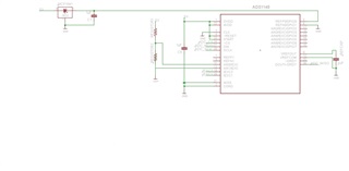
  •  I am using  ADS1148Q1 IC and applying analog input of 0V to +5V from a potentiometer, connected to an AN0 pin, all other analog input pins are grounded
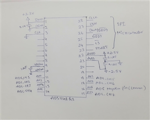
     

    Code I used <>

    //1) CRO check on DRDY pin
    //2) SCK pin data check
    //3) RESET pin connected to digital pin


    #include <SPI.h>
    int a = 555;
    const byte READ = 0b11111111;
    #define RESET 7 //reset pin
    #define START 8 //start condition pin
    #define DRDY 9 //data ready pin
    float d, e;
    float average;
    int cnt;
    void setup()
    {
    Serial.begin(115200);

    pinMode(START, OUTPUT);
    pinMode(RESET, OUTPUT);
    pinMode(DRDY, INPUT);

    digitalWrite(RESET, HIGH);

    digitalWrite(START, HIGH);//this is for start conversion pin to initiate the conversion start
    SPI.begin();

    digitalWrite(SS, LOW);
    SPI.transfer(0x06);
    delay(1);
    SPI.transfer(0x16);
    SPI.transfer(0x40);
    SPI.transfer(0x0E);


    SPI.transfer(0x01); //MUX0 
    SPI.transfer(0x00); //VBIAS
    SPI.transfer(0x30); //MUX1
    SPI.transfer(0x08); //SYS0
    SPI.transfer(0x00); //OFC0
    SPI.transfer(0x00); //OFC1
    SPI.transfer(0x00); //OFC2
    SPI.transfer(0x00); //FSC0
    SPI.transfer(0x00); //FSC1
    SPI.transfer(0x40); //FSC2
    SPI.transfer(0xA0); //IDAC0
    SPI.transfer(0x00); //IDAC1
    SPI.transfer(0x80); //GPIOCFG
    SPI.transfer(0x00); //GPIODIR
    SPI.transfer(0x80); //GPIODA

    digitalWrite(SS, HIGH);
    delay(10);

    digitalWrite(SS, LOW);

    SPI.transfer(0x20); //Read starting from address 0
    SPI.transfer(0x0E); //Read 0xE + 1 = 15 bytes
    uint8_t MUX_0 = SPI.transfer(0xFF); //Read Mux0
    uint8_t VBIAS = SPI.transfer(0xFF);
    uint8_t MUX_1 = SPI.transfer(0xFF);
    uint8_t SYS0 = SPI.transfer(0xFF);
    uint8_t OFC0 = SPI.transfer(0xFF);
    uint8_t OFC1 = SPI.transfer(0xFF);
    uint8_t OFC2 = SPI.transfer(0xFF);
    uint8_t FSC0 = SPI.transfer(0xFF);
    uint8_t FSC1 = SPI.transfer(0xFF);
    uint8_t FSC2 = SPI.transfer(0xFF);
    uint8_t IDAC0 = SPI.transfer(0xFF);
    uint8_t IDAC1 = SPI.transfer(0xFF);
    uint8_t GPIOCFG = SPI.transfer(0xFF);
    uint8_t GPIODIR = SPI.transfer(0xFF);
    uint8_t GPIODAT = SPI.transfer(0xFF);
    digitalWrite(SS, HIGH);
    delay(5);
    digitalWrite(SS, LOW);
    SPI.transfer(0x04);
    delay(1);//SYNC Command
    digitalWrite(SS, HIGH);
    }

    void loop() {

    if (digitalRead(DRDY) == LOW) {

    digitalWrite(SS, LOW);
    delay(7);
    SPI.transfer(0x12);
    delay(1);
    unsigned int high_byte = SPI.transfer(0xFF);
    delay(1);
    unsigned int low_byte = SPI.transfer(0xFF);
    delay(20);
    digitalWrite(SS, HIGH);

    unsigned int adc_data = (((uint16_t) high_byte) << 8) | ((uint16_t) low_byte);
    Serial.println((adc_data * 4) & 0xFF00);
    delay(500);
    }
    }

  • Hi Vivek,

    Thanks for the additional information.

    The ADS1148-Q1 does not support ground-referenced inputs with a unipolar supply. Please refer to Equation 3 in the ADS1148-Q1 datasheet for more information. Therefore, your configuration is not valid, and you instead should be taking measurements on the high side of the resistor divider (pot), not the low side.

    Also, keep in mind that the ADS1148-Q1 has a bipolar coding scheme. Therefore, the ADC output codes span from -FS to +FS, or -VREF/gain to +VREF/gain. When you set MUX1 = 0x30h, that is 0011 0000b which selects the ADC's internal 2.048V reference. SYS0 is 0000 1000b, which selects a gain of 1 and a data rate of 1000 SPS. This establishes an ADC output code span of -2.048V to +2.048V. However, you are inputting 0-5V, so you can see how you will not be able to realize the ADC's entire full-scale range (# of bits). Please remedy these issues and you should see better results.

    I will also point out that the external reference you are using (MCP1541) is a 4.096V reference. However, the max differential reference voltage you can apply to the ADS1148-Q1 is AVDD - AVSS - 1V, which in your case is only 4V. Even though it is close, you are operating the ADC outside of its recommended conditions when using a 4.096V reference. Please keep this in mind if you do intend to use an external reference.

    -Bryan

  •   Hi Bryan,

    I did this Circuit for my 7 channel BIpolar ADC input voltage range from -2.5V to +2.5V.

    I am not able to read data from channels, Please help me out with any other solution, I am not able to identify any problem in this circuit neither in the code.

    given power supply

    AVDD +2.5V, AVSS -2.5V

    DVDD +3.3

    //code for reading data from channels
    //ARDUINO UNO board

    #include<SPI.h>
    uint8_t high_byte[16];
    uint8_t low_byte[16];
    uint16_t adc_data;
    uint8_t data_ready;
    uint8_t received_val = 0;

    #define RESET 7 //reset pin
    #define START 8 //start condition pin
    #define DRDY 9 //data ready pin

    void setup() {
    Serial.begin(9600);
    pinMode(RESET, OUTPUT);
    pinMode(START, OUTPUT);
    pinMode(DRDY, INPUT);
    digitalWrite(RESET, LOW);
    delay(10);
    digitalWrite(RESET, HIGH);

    delay(16);
    SPI.begin();

    digitalWrite(SS, LOW);
    delay(16);
    SPI.transfer(0x06);
    delay(1);
    SPI.transfer(0x14);// Selected Contineous data read mode 7 channels

    SPI.transfer(0x40);
    SPI.transfer(0x0E);
    SPI.transfer(0x00); //MUX0
    SPI.transfer(0x00); //VBIAS
    SPI.transfer(0x30); //MUX1
    SPI.transfer(0x52); //SYS0
    SPI.transfer(0x00); //OFC0
    SPI.transfer(0x00); //OFC1
    SPI.transfer(0x00); //OFC2
    SPI.transfer(0x00); //FSC0
    SPI.transfer(0x00); //FSC1
    SPI.transfer(0x40); //FSC2
    SPI.transfer(0x06); //IDAC0
    SPI.transfer(0x89); //IDAC1
    SPI.transfer(0x80); //GPIOCFG
    SPI.transfer(0x00); //GPIODIR
    SPI.transfer(0x80); //GPIODAT
    digitalWrite(SS, HIGH);
    delay(10);

    digitalWrite(SS, LOW);


    SPI.transfer(0x20); //Read starting from address 0
    SPI.transfer(0x0E); //Read 0xE + 1 = 15 bytes
    uint8_t MUX_0 = SPI.transfer(0xFF); //Read Mux0
    uint8_t VBIAS = SPI.transfer(0xFF);
    uint8_t MUX_1 = SPI.transfer(0xFF);
    uint8_t SYS0 = SPI.transfer(0xFF);
    uint8_t OFC0 = SPI.transfer(0xFF);
    uint8_t OFC1 = SPI.transfer(0xFF);
    uint8_t OFC2 = SPI.transfer(0xFF);
    uint8_t FSC0 = SPI.transfer(0xFF);
    uint8_t FSC1 = SPI.transfer(0xFF);
    uint8_t FSC2 = SPI.transfer(0xFF);
    uint8_t IDAC0 = SPI.transfer(0xFF);
    uint8_t IDAC1 = SPI.transfer(0xFF);
    uint8_t GPIOCFG = SPI.transfer(0xFF);
    uint8_t GPIODIR = SPI.transfer(0xFF);
    uint8_t GPIODAT = SPI.transfer(0xFF);
    digitalWrite(SS, HIGH);

    digitalWrite(SS, LOW);
    SPI.transfer(0x04);
    delay(10);
    }

    void loop() {
    digitalWrite(START, HIGH);
    delay(10);
    digitalWrite(START, LOW);
    data_ready = 1;
    delay(1);
    while (data_ready == 1)
    {
    data_ready = digitalRead(DRDY);
    }

    for(int i=0;i<15;i++)//for reading 14 bytes of 7 channels data
    {
    digitalWrite(SS, LOW);//low slave select pin
    delay(7);
    // SPI.transfer(0x12);
    high_byte[i] = SPI.transfer(0xFF);
    low_byte[i] = SPI.transfer(0xFF);
    delay(20);
    digitalWrite(SS, HIGH);
    adc_data[i] = (((uint16_t) high_byte[i]) << 8) | ((uint16_t) low_byte[i]);//data stored on array
    Serial.print(adc_data[i]);//adc data print
    }
    }

  • Hi Vivek,

    Can you provide logic analyzer data or oscilloscope shots of the SPI transactions for your system? If something is wrong with the communication, this will be the best way to diagnose the issue. Please include DIN, DOUT, SCLK, CS and DRDY while you are reading and writing to the device. This will help us understand if the SPI timing is correct as well as if the correct commands are being issued and understood by the ADC.

    -Bryan