Hi,
I'm still using your ADS1675 (wonderful device) in another new project.
In the past projects, I was using the device as low-speed (1MSPS), 32MHz external clock, CMOS output interface, but in this new one I have to select the datarate among 1MSPS and 2MSPS.
To simplify the FPGA design, I've decided to use LVDS interface and internal SCLK generation for both application.
General settings (hard-wired) are the following:
CS = '0' (single device); SCK_SEL = '0'; LVDS = '0'; LL_Config = '1'; FPATH = '0'.
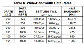
The DRATE is set to '011' for 1MSPS and to '100' for 2MSPS.
The START pin is "strobed" at each configuration changes and then keep high for continuous acquisition.
For 1MSPS, the CLK provided to ADS1675 is 24MHz that, with internal PLL x1, provide a correct 24MHz on SCLK pin.
For 2MSPS, the CLK provided is 16MHZ that, with ionternal PLL x3, provide a correct 48MHz on SCLK pin.
To test the design we provide an analog continuous sinusoidal waveform of 50 KHz.
When we dump the samples,the recovered waveform seems correct for both bitrates.
But we have unexpected behaviour on DRDY timing.
As showns by jpg DRATE_3 (datarate = '011', 1MSPS), we observes that the timing at which DRDY occurs, is ~ 1.3us instead of 1us (32 SCLK cycles at 24MHz instead of 24).
As showns by jpg DRATE_4 (datarate = '100', 2MSPS) the rate at which DRDY occurs is 1us (48 SCLK cycles instead of 24).
We have also tested it in a different setting, as you may see in the jpg DRATE_5.
In this case the DRATE is '101', that correspond to 4MSPS, but we still provide 16MHz on CLK pin.
As you may see, this setting seems to correspond to a correct 2MSPS behaviour: the SCLK pin is 48MHz, the occurrence of DRDY is 0.5us and the numlber of SCLK cycles to the occurence of DRDY is 24.
Whgat have we missed out ?
Thanks in advance
Andrea