This thread has been locked.

If you have a related question, please click the "Ask a related question" button in the top right corner. The newly created question will be automatically linked to this question.

BP-DAC81404EVM/BP-DAC61402EVM GUI runtime error

Other Parts Discussed in Thread: UNIFLASH, DAC81404EVM, DAC81404

I followed user guild for BP-DAC81404EVM, BP-DAC61402EVM.

In 2.1.1 Software Installation,

The EVM software is compatible with the Microsoft® Windows® 7, 8, and 10 operating systems. The
software is found in the GUI Composer Gallery. Search for BP-DAC81404EVM or BP-DAC61402EVM in
the GUI Composer Gallery. Use the down arrow symbol to download the software. There are two
downloads: BP-DAC81404EVM or BP-DAC61402EVM GUI and the respective GUI Composer Runtime.
Either download both, or just download the EVM GUI; the runtime file can be downloaded through the
EVM GUI during installation. The software can also be run online; however, only after the firmware and
driver are upgraded. After the software is downloaded onto the PC, navigate to the download folder, and
run the BP-DAC81404EVM or BP-DAC61402EVM software executable...

My problem is that I have downloaded GUI runtime for the EVM board. However, when I run it, it gives me error as showed below:


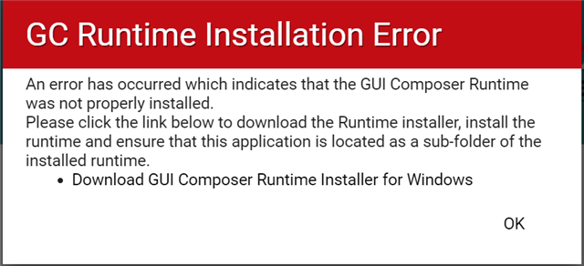
Anyone ran into this before? Any solution?

  • Hi he dajiang, 

    In the MSP interface headers, as shown in the user manual, you can find the relevant pins. 

  • Hi,

    Any update? Do you need more help?

    Regards,

    AK

  • Yes, I've been trying to use Arduino UNO to communicate with 81404 EVM board.

    For jumper, I use default settings as in Table 6.

    For Launchpad interface pins:

    EVM board             UNO

    3.3v           <-->      3.3v 

    5v              <-->      5v

    LDAC        <-->      6  LDACz_PIN

    SYNC        <-->      10  DAC_SS_PIN

    SDIN        <-->      11  MOSI

    SDO        <-->       12 MISO

    SCLK       <-->      13 SCLK

    CLR, RST <-->      5  DAC_RESET_PIN

    This is my Arduino code for set up, which I copied from Parswa's post.

    // Chip Select
    pinMode(DAC_SS_PIN, OUTPUT);
    digitalWrite(DAC_SS_PIN, HIGH);

    // reset
    pinMode(DAC_RESET_PIN, OUTPUT);
    digitalWrite(DAC_RESET_PIN, LOW);
    delay(10);
    digitalWrite(DAC_RESET_PIN, HIGH);
    delay(10);

    // LDACz_PIN
    pinMode(LDACz_PIN, OUTPUT);
    digitalWrite(LDACz_PIN, LOW);

    // Init SPI0
    Serial.println("SPI0 init...\n");
    SPI.begin();
    delay(100);

    // Write
    write_reg(0x03, 0x0A84); // SPICONFIG: DEV-PWDWN=0
    write_reg(0x04, 0x0); // GENCONFIG: REF-PWDWN=0
    write_reg(0x09, 0x0); // DACPWDWN: DACx-PWDWN=0, x={A,B,C,D}
    write_reg(0x05, 0x0); // BRDCONFIG: DACx-BRDCAST-EN=0
    write_reg(0x0A, 0x5555); // DACx-RANGE=0b0101, i.e. +/-5V

    Function write_reg is exactly the same as Parswa's.

    In the loop, I have

    uint16_t i = 65000;
    void loop() {
    // put your main code here, to run repeatedly:

    write_reg(0x10, i%65535 ); // DAC-A
    write_reg(0x11, i%65535 ); // DAC-B
    write_reg(0x12, i%65535 ); // DAC-C
    //write_reg(0x13, (4*i)%65535); // DAC-D

    //i = (i+64)%65535;
    //delayMicroseconds(5);

    read_reg(0x01);
    delay(60000);
    }

    However, I still cannot detect any voltage from TP2,4,5 to GND.

    I have another issue, I tried to read register value (DEVICEID) from 0x01, only to get 0xFF.

    Here is my code to read:

    SPI.beginTransaction(settingsA);
    CSON();
    delayMicroseconds(1);
    // first bit 1 is to read
    SPI.transfer(reg & 0x80);
    SPI.transfer(0x00);
    SPI.transfer(0x00);

    // 3 more bytes cycle to read
    uint8_t val1 = SPI.transfer(0x00);
    uint8_t val2 = SPI.transfer(0x00);
    // We want only last byte
    uint8_t val3 = SPI.transfer(0x00);
    delayMicroseconds(1);
    CSOFF();
    SPI.endTransaction();
    //Serial.println("Device ID ");
    Serial.println(val1, HEX);
    Serial.println(val2, HEX);
    Serial.println(val3, HEX);

  • Hi,

    Can you post the SPI frame for the function

    write_reg(0x03, 0x0A84);

    I need SYNC, SCLK and SDIN scope shots

    Regards,

    AK

  • I don't know why I cannot continue to add reply to your latest post. So I have to reply my first post.

    Using scope will be my last resort, which I can only do on Wednesday. Tomorrow I cannot come back to office because of COVID protocol.

  • Hi,

    That's because the thread has become too large. No problem, you can always reply to the first, web page will always show it correctly.

    Now, please provide us with the scope shots for the debug. What is the SPI mode you are operating?

    Regards,

    AK

  •   

    Blue line: Chip select, Yellow: clock. Right side: zoomed in

    I guess the issue is there is a gap between each byte. 

    Yellow: Clock signal. Blue: MOSI/SDIN.

    BTW, High signal from Arduino UNO is 5V. Is 81404 OK with that?

  • Hi,

    5V logic is fine, no issues

    Also SCLK gap is ok, Can I get all three of them together? SYNC, SCLK and SDI to get the timing correct?

    Which SPI mode are you using from your Arduino? Our device supports Mode 1 and 2

    Regards,

    AK

  • I borrowed Parswa's code, in which he used mode 0. Strangely he said it was working for him.

    OK, later I will change to mode 1 to try.

  • The above 2 figures show the signals of 3 SPI pins (top: clock; middle: data; bottom: CS) for writing 0x0A 0x84 to register 0x03.

    The data and clock look OK. Only the CS has a few spikes, which can be ignored. I just found out that my GND pin is wired wrongly.

    SPI setting is showed below. Here I use a STM32 development board.

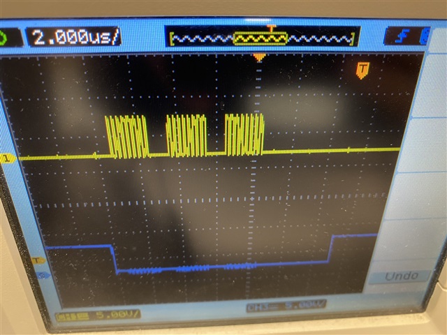
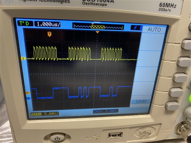
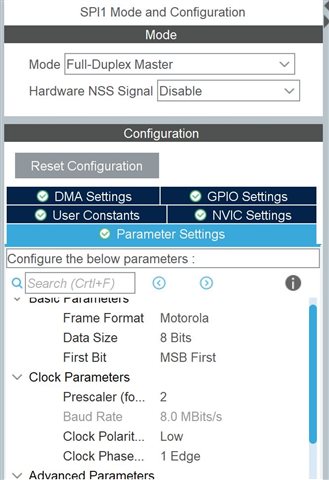
       Does the SPI frame looks OK?
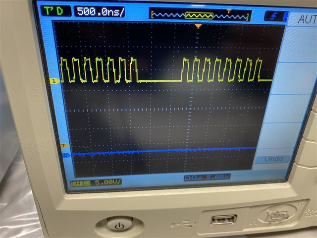
    I also want to know if my register-reading code is OK. After MOSI sends out 3 bytes reading command, it continues to send 3 dummy bytes and in the mean time MISO reads 3 bytes.

  • Hi,

    CS line has to be kept low for 3 bytes of write. In your diagram, I can see CS going high in between transactions which is not correct.

    Device will ignore these bytes. Please make sure that CS signal low.

    Regards,

    AK

  • Finally I got voltage output after I connect DAC_VDD of J17 pin 1 to a power supply. Previously I thought 3.3 and 5v power supply from its launchpad interface would be enough.

    Now my question is whether the stability of its voltage output depends on external power supply. Hopefully not.

  • Hi,

    Stability of output voltage depends on DAC reference voltage, AVDD and AVSS power supplies.

    Are you driving any capacitive load on the DAC output?

    Regards,

    AK

  • My setup works perfectly as expected. There's a Fast SDO (FSDO, enables half cycle speedup) bit in the SPICONFIG register. Page 3 of the datasheet reads:

    "Data are clocked out of the input shift register on either rising or falling edges of the SCLK pin as specified by the FSDO bit (rising edge by default)."

    Then page #36, you will find: 

    "Fast SDO bit (half-cycle speedup). When 0, SDO updates on SCLK rising edges. When 1, SDO updates on SCLK falling edges."

    If you see my code, the initialization function sets the FSDO bit to 1. i.e. 

    // set SPICONFIG: DEV_PWDN=0, FSDO=1
    uint16_t def = TEMPALM_EN(1) | DACBUSY_EN(0) | CRCALM_EN(1) | DEV_PWDWN(0) | CRC_EN(0) | SDO_EN(1) | FSDO(1) | (0x2 << 6);
    write_reg(R_SPICONFIG, def);

    This is why I use SPI mode 0 (see Introduction to SPI Interface from Analog Devices, Table 1). 

  • Hi

    This device supports SPI mode 1 and 2 for data writing. Please see the timing diagrams. Idle state of clock polarity can be high or low, but data is always sampled on falling edge of SCLK and SDO can be either ways based on FSDO.

    Regards,

    AK

  • Hi Akhilesh, can I check with you: for SPI CS line, as long as it is low, 81404 will receive data; or it must go from high to low to trigger?

  • Hi,

    /CS (SYNC) pin must stay low for minimum 24 SCLK edges to receive the data by DAC81404. DAC update can occur in 2 ways. If the device is in synchronous mode, writing to the DAC data register does not automatically update the DAC output. Instead the update occurs only after a trigger event. A DAC trigger signal is generated either through the SOFT-LDAC bit or by the LDAC pin. The synchronous update mode enables simultaneous update of multiple DAC outputs.

    In asynchronous mode, a DAC data register write results in an immediate update of the DAC active register and DAC output on a /CS rising edge.

    As a summary, in both modes, /CS has to go high for the DAC update to occur. Synchronous mode is helpful when you want to update multiple channels at once.

    Regards,

    AK