This thread has been locked.
If you have a related question, please click the "Ask a related question" button in the top right corner. The newly created question will be automatically linked to this question.
From the ADS1298 Datasheet
"After eight serial clock events, the ADS1294/6/8 assumes an
instruction must be interrupted and executed. If it is suspected that instructions are being interrupted erroneously,
toggle the chip select pin high and back low to return the chip to normal operation. It is also recommended to
issue serial clocks in multiples of eight. "
Can someone please clarify whether I should Take CS High between every 8 cycles or not?
I'm trying to read the id register. But have been unable to till now.
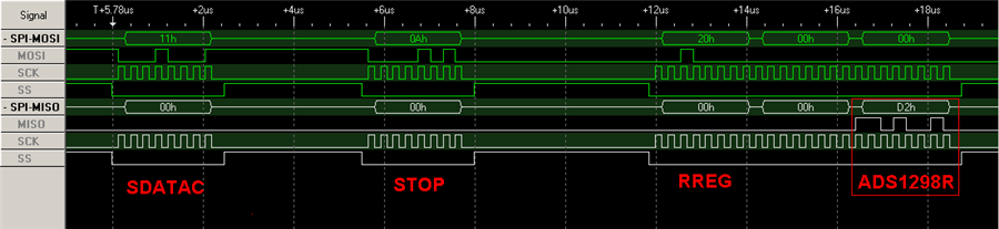
SPI Sequence =
CS low
06h (Reset)
CS high
Sleep 1000ms
CS low
11h (SDataC)
CS high
Sleep 1ms
CS low
20h (Read ID Reg)
CS high
Sleep 1ms
CS low
00h (Read only one reg)
CS high
sleep 1 ms
CS low
00h (Dummy. to read ID reg)
CS high
I always get 00h.
Is something wrong with the above algorithm?
Regards
Zubair
**TI EDIT February 20th 2019; FOR GENERAL ADS129x ASSISTANCE, PLEASE SEE NEW BIOPOTENTIAL FAQ LOCATED HERE**
Hi Zubair,
On page 40 of the datasheet for the ADS1298 the conditions for the /CS input are described in better detail. For single byte opcode commands, the /CS input can toggle between the eight SCLKs issued for that command - for instance with WAKEUP or SDATAC. With multi-byte commands, like RREG, the /CS must be low for the entire 24 clocks. Since a picture is worth 1000 words, please have a look at this screen capture we took from the ADS1298R.
Please let us know if this helps to clarify what you need to do to read the register ID bits.
I was able to read the Device ID register successfully.
Thanks again for the CS info.
If its not too much of a bother, can someone please upload a screenshot(s) like the one above for
a basic read from a channel as well. Test signal configuration. Or even normal electrode configuration.
Read Single Byte and Multi Byte.
The screenshots will be a big help to everyone here.
Regards
Zubair
Great! Glad to hear you've got the device ID! Since there really is no 'single byte' read option, I can't give you an example there - essentially that would be one of the single byte opcode commands above. Since this is a synchronous serial interface, technically a single byte write is also a single byte read as well. Here are a couple more screen captures for you though.
This one shows the command cycle for the 'test signals' to be applied to the input mux:
This one is for the 'Normal Electrode' configuration:
And this one is a read back of the Status, CH1 and CH2. Please note the addition of the DRDY signal here. The software associated with our ADS1298 hardware uses the DRDY as an interrupt. When data is available, DRDY goes low and returns high again after seeing the first SCLK from the host processor.
Let me know if you find these useful or if there is anything else you want to see.
Thanks for the screenshots. They are a big help.
I've been able to read and write the configuration registers successfully thanks to them.
Had to introduce a delay between each opcode. Missed it in the datasheet. Our code didn't work.
The delay was visible in the screenshot. After including the delay, it worked. :)
I have gpio's and was thinking to use them for data acquisition. Using Powerdown, Start and Reset on the pins
instead of the opcodes. Any chance you can reproduce the third screen shot with the pins as well?
The flow chart at the end of the datasheet is confusing. Like you said. A picture is worth a thousand words.
A screenshot of the flowchart implementation or even better. A normal data-acquisition start-up sequence.
With the pins instead of opcodes if possible.
That would be really great!
Regards
Zubair
Hello there,
I'm having a similar problem to the one you had, Zubair. I created a reading/writing function some time ago but this time I tried to use it. It didn't work. So I'm trying to do it register by register. So far I was able to read the ID register but I slightly modified the code and now it's gone again. The thing's that right now I'm doing it without the /CS toggling, which makes it kinda tricky (kinda like blindfold) to set the transmission properly as you need it to be in multiples of 8tclks. Therefore, I'm interested to now how did you set up the /CS toggling. Because so far I have tried to set it up similar to what you have at the beginning, but apparently when I toggle the /CS back to 0 to process the command, MISO/MOSI remain in what I think is high impedance state; either 0xFF or 0x7F, for either Open drain or push-pull pin configurations.
I would really appreciate if you could comment on the /CS toggling, maybe I'm missing some particular delay (apart from the one between commands which I have).
An qualitative answer would be nice for the beginning. Later I can elaborate further on it.
Thanks
I just pulled the CS low permanently and forgot about it. It kinda worked. I only had one ADC on the SPI bus..
I don't understand what you mean by transmission needs to be in multiples of 8tclks..
Regards
Zubair
Ah, ok, so you went for the constant /CS=0 method. I just thought the toggling one was quite elegant and more precise, because if you just add some delays between commands it can be the case (as has happened to me) that you lose synchronization and you have to reset the SPI to get to normal state again. What I meant with transmission in multiples of 8sclks (not tclks...my bad) was that as the SCLK issues 8 clock cycles per command, so in order to keep the interface synchronized it is desirable that the serial transmissions always take place in multiples of 8sclks, otherwise it could be that you start already half way through some clock pulse and/or out of phase. So far I tried with the toggling method and it seems to work, though some times it loses coherence somehow. I guess there must be some glitches. Does it work smoothly for you every time? or do you have to reset after certain amount of time?
Regards,
Gilbert
I'm not sure. But every once in a while. It would glitch. could be just cause of a bad trace. But I'd acquire 40,000 samples.
And had written the code to reset and reconfigure it every time it after that. No more glitches.
Also, if i remember correctly, using RDATAC would glitch a lot. Sending RDATA every time would not glitch.
Regards
Zubair
Hello Tom,
I'm currently working with the ADS1298 (Controlled by a C8051F342 uc). So far, I succesfully read the ID register and I've been able as well to read and write other registers. There's only one thing puzzling me. When I send the first command to the ADS (SDATAC in your diagram) I read sometimes 06h instead of reading 00h, the rest of the steps complete flawlessly, but I just thought that It shouldn't be the case that you read some value at first as the SPI is supposed to be empty. What's funny is that even if I start with another command, say RESET, I get the same behavior: I read 06h in the first command and all of the rest are ok.
This fact lead me to think that it is maybe that the chip select needs some delay before starting the transmission, but so far even with different delays I still get the same behavior. The problem corrects if I unplug everything and connect again, so one could suspect it is more on the microcontroller side. But I just wanted to ask you if you have so far experienced something similar maybe with other microcontrollers or if it's maybe a typical set up problem.
Looking forward to hearing from you
Santiago
Hiren, Saloni,
Please refer to the datasheet for the ADS1298. That document contains the comprehensive explanation of details of the chip's operation - including how to interface with the device.
Regards,
Brian Pisani