


I have two ADC interfaces(ADS5562 and ADc4128) with FPGA and 32-bit processed output data from FPGA.
I have an IO signals to verify the Inputs and Outputs of FPGA.
But I don't have any test points to verify the intermediate output blocks of the design like mixer and filter. Since I need to cross check the functionality of mixer and filter also either its meeting my requirement or not. What is best method to evaluate the functionality of complete blocks along with intermediate blocks.
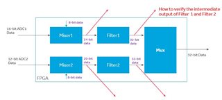
I have following doubts with respect to the above block diagram.
1. Either I am doing right or Is there any best solution to verify the intermediate blocks of design along with actual IOs. Actual blocks of the design is mentioned in the attached figure.
2. If I have a 40K samples its very difficult to fed either in simulation or On-board testing, how to give this huge samples as part of simulation or ON-board Testing ?
3. what is the Idle way to verify the Signal processing chain in Simulation and On-board testing.
4. How to verify the build in test operation of ADS5562. Since it doesn't have any SPI read operation support.
