This thread has been locked.

If you have a related question, please click the "Ask a related question" button in the top right corner. The newly created question will be automatically linked to this question.

TSW14J56EVM: FPGA upgrade

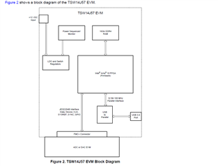
Part Number: TSW14J56EVM

Dear Support/Expert

I am working on a project to migrate the TSW14J56EVM Arria V FPGA to Arria 10. I understand it is not TI's responsibility to support this migrate, but I think I may not be the only one has this kind of request. it may help all the designers that need to use newer FPGA. so I am asking for any suggestion/idea to make this migration a little easier, on battle field, a word from veteran could save a life. here a few words may save new one's weeks or month of time. 

Sincerely

David

  • David,

    TI has a TSW14J57EVM that uses the Arria 10 device. Would the source code for this board help you?

    Regards,

    Jim

  • Really, I got the project in the middle with a TSW14J56 board, so I didn't have much early investigation. let me have a look at the TSW14J57 on TI's website, the company I served do have NDA with TI, if the source code need NDA, I can ask for a copy, otherwise, please send me a copy. 

    it is really a surprise to me. thank you very much.

  • by the way, is this TSW14J57EVM support AFE58JD48, from the document of AFE58JD48, it didn't mention TSW14J57EVM. did I miss anything when I read the document?

  • Example source code can be downloaded from the following link:

     https://tidrive.ext.ti.com/u/xdnJpu7ZyZ7X2cmn/fb7b0f39-7b24-4369-9687-90b2483a166a?

    The TSW14J57 does not currently support the AFE58JD48.

  • Thank you very much, we need to implement PCIe interface anyway. is there any other example Arria 10 project that instantiate PCIe in it? it is much faster to do a new design with an example/template. appreciate your help.

  • did I miss anything here, the list price of the TSW14J57EVM on TI is only $1,999. from the BOM this FPGA is 10AX115H1F34E1SG, this chip only with cost $7,842.05 at Digikey. 

    I am so confused,  we can use this chip if it almost $8000 each. how can TI make the EVM so cheap?

  • We are advertising their device with our EVM so we are getting a discount.

  • Hi Jim, 

    I think the develop will start from porting the FPGA to a lower cost Arria10 like 660( Intel develop board a10_soc_devkit_03_31_2016). Because it is from the same family, may be it won't be very difficult. What I think the most challenge is that the design is targeting use 2 or more AFE58JD48. even I study AFE58JD48EVM very carefully and understand it, but there didn't mention much of the integration and synchronization multi chips. could you please give me some link or any kind of suggestion to dig out more detail and reference before I start the design. for a complicate design like this, any small mistake will cost tens of thousands of dollar and weeks of time. 

    by the way, is it possible or realistic for us to build an AFE board, with 2 TX7516 and 2 AFE58JD48 with a FMC port that compatible with the TSW14J57EVM. will it be a little easier to develop FPGA and PC software based on the TI's J57 platform.

    Appreciate your help

    Best Regards,

    David  

  • David,

    This part is supported by our medical group which I will forward this post to. They should be able to answer questions regarding the AFE device. 

    Regards,

    Jim 

  • Hi Jim, 

    Is the project in the above link called J57_ADC12DJ5200_10p4G.qar? if yes, then this is only an example to instantiate a JESD. there is not glue logic and the interface to the DDR and USB. 

    if not, it is possible that after I download the link above and I forgot where I put it. could you please send me the link again, thank you.

  • Hi Jim

    from the "TSW14J57 JESD204B High-Speed Data Capture and Pattern Generator Card User's Guide"(SLWUA,here is the EMV block diagram. it is very similar to the architecture of TSW14J56.  but the FPGA package I download from your provided link is far away from this architecture. 

    the next picture is I put the two project Hierarchy side by side. from TSW14J56 project, there are function blocks like fx3_main for USB3.

    ddr3_emif for the DDR. and Avalon bridge.  but the project from TSW14J57, only provide a JESD module. and in the top level .v file. there instantiate two altera_jesd204 u0_jesd204 modules, but has a note like this

    "  //JESD Base IP for RX
    //JESD Avalon slave is not used. All the slave signals are made inactive"

    as a newbie to the JESD, the J56 has everything but based on Arria V, I have tried to upgrade to Arria10, but it is not very straight forward. there are lot of IP cores need to be created for the new chip.

    The J57 EVM seems is the right example on right chip, but it only covered a small portion of the board function. 

    I didn't expect a plug and play example, but I hope I can get as much as possible of a project like the block diagram. So I can focus on how to apply the function blocks instead of learn how to generate each IP and how to connect them together. 

    Could you please provide another example project that similar to J56 but for Arria 10 device?

    thank you very much!

    David

  • Hi Jim, 

    Do you have time to have a look at my post about a week ago? the link you provide me is just a small potion of the whole PFGA function, Did I miss anything? Is there a package that contains more features of the block diagram( like emif and usb3 interface?

  • David,

    You can download more info from the link below. I also attached a couple of files.

    Regards,

    Jim

    tidrive.ext.ti.com/.../7a0a22dd-4d97-4fad-91c4-a8d60951de80

  • Hi Jim, 

    this link is different to the last one, it need different account to the TI support Forum, for some reason, the Authentication or authorization failed. do I need apply a TI Enterprise account to download it. 

    Thanks,

    David