This thread has been locked.

If you have a related question, please click the "Ask a related question" button in the top right corner. The newly created question will be automatically linked to this question.

ADS124S08: Unable to control two ADC IC using CS (chip select) pin.

Part Number: ADS124S08

Hi All,

We are using ADS124S08 IC in one of our project. We are facing some communication issues with Chip Select (CS) pin. When we directly connect the CS pin to DGND (means we have connected CS pin to DGND using external jumpers) the IC works fine and we able to read all the 12 channels (single ended) properly.

We are using Raspberry PI compute module (CM-4) to communicate with ADS124S08. And when we tied CS pin (of ADC) to CM-4 Chip select pin we are not getting proper reading (it showing garbage values of 0-2mV) where the actual Input signal on AIN pins was 0.5V-2V.Gain is set to 1.

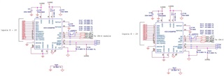
In our project we have used two ADS124S08, if we forced ground first ADC IC using Jumper J1=closed & J2=open (schematic attached) the First IC works fine but the other one gets inactive and vice versa. Our Aim is to get the readings from both the ADC ICs and It will be possible only if we able to control/toggle CS pin of both from GPIO pins (not by physical ground).

While getting garbage data, we even tried giving Reset to ADC (by connecting RESET pin to ground ) but we still getting wrong data. Until we power reboot the entire device (with CS pin connected to ground).

Things we tried are as follows.

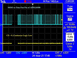
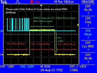
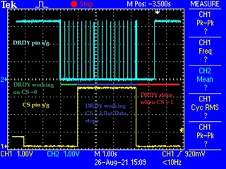
a. We check our signal on CS pins on Digital Oscilloscope, when its LOW it is giving proper 0V and on HIGH it is 3.3V.

b. We tried giving CS signals from other available GPIO pins on CM-4 module.

c. Connect Pull down resistor 10k & 4.7K (one at a time) to CS pin.

d. Tried controlling CS pin using NPN transistor (BC847).

Are we missing any register reading/writing, Reading sequence, Timing, or any hardware point etc.

Please suggest. Thanks in advance

  • Hi Gulam,

    Welcome to the E2E forum!  One common mistake that is made is not keeping CS low throughout the entire communication transaction.  Usually this requires a GPIO to go low at the beginning of the communication and then go high once the communication is completed.  If the CS toggles after a byte is read or at anytime during the communication cycle, the rising edge of CS will cancel the communication.

    Can you send communication plots from an oscilloscope or logic analyzer for me to review?  Please include all signals such as CS, DOUT, DIN and SCLK.

    You might want to verify that CS is working as intended at the ADS124S08 CS pin.  There could be something wrong with the way you implemented the jumper and perhaps the pin is floating and not truly connected to the micro.

    Best regards,

    Bob B

  • Hi Gulam,

    Were you able to capture shots of the communication for me to review?  

    Best regards,

    Bob B


  • Myself Kamil H Shaikh,colleague of Gulam,Sir Please help us,we are stuck,
    Chipselect issue,PFA the images & description

    IC:ADS124S08

    Platform: Raspberry Pi CM4 (BCM2711)
    Application:We need to Access 2 X ADC(ADS124S08) with same SPI bus and different Chipselect CS0 and CS1,
    With total 12 X 2 = 24 channels to be read.

    Hardware Scenario:

    We are not using DRDY pin,By default we have kept
    RESET = 1,Pull Up to 3.3Vcc by 4.7kohms
    START/SYNC = 0,pull down to grnd by 4.7kohms
    CLK = 0,directly at Grnd since we are using Internal Oscillator
    DRDY pin we are not using.
    AINCOM = AVSS = IOVDD = common grnd
    Voltage reference: Internal 2.5V
    for other pins please refer schematic screen shot.

    Observations:We are able to successfully write & Read all 18 regsiters with CS tied to grnd,
    Also 12 Channel are successfully being read with speed of 80ms(Time delay for each Channel) X 12 Channel.
    In all all channels are being read at interval of approx 1 second.


    Please Refer image 004-a.Jpg
    Action 1:CS tied to Gnd,works fine as stated above.

    Action 2: CS = 0 on Power ON
    Now instead of GND we use GPIO for CS as intended,
    So On power on we keep CS = 0,due to which IC serial port gets active,
    Accurate data is recieved.This CS = 0 is kept for 20 seconds,by code
    DRDY is seen toggling on DSO.

    Action 3:CS = 1 after action 1 in code continuation the program make CS = 1
    for 20 sec,for which no data must be seen on MISO as intended.OK-No problem
    DRDY is OFF(Logic 0)

    Action 4:In continuation after Action 3,program makes CS = 0,for next 20 sec
    now here its intended that the MISO or Data out pin must start the data stream,
    but No data starts.Serial SPI ports get inactive to any command only 0x00,0x00,
    0x00 is recieved.
    DRDY is OFF(Logic 0)

    Commands:-
    #define CMD_NOP 0x00
    #define CMD_WAKEUP 0x02
    #define CMD_PWRDWN 0x04
    #define CMD_RESET 0x06
    #define CMD_START 0x08
    #define CMD_STOP 0x0A
    #define CMD_RDATA 0x12


    Configuration Register Values

    DEV_ID= 0x80;
    STATUS= 0x00;
    INPMUX= 0x0c;

    PGA= 0xA0;
    DATARATE= 0x9D;
    REF= 0x3A;

    IDACMAG= 0x00;
    IDACMUX= 0xFF;
    VBIAS= 0x00;

    SYS= 0x1B;
    OFCAL0= 0x00;
    OFCAL1= 0x00;

    OFCAL2= 0x00;
    FSCAL0= 0x00;
    FSCAL1= 0x00;

    FSCAL2= 0x40;
    GPIODAT= 0x00;
    GPIOCON= 0x00;

    Note:Code Sequence not actual code:-

    UINT8 Loop=0
    1. CS = 0
    2. CMD_RESET is sent by SPI
    3. WREG 18 register //Works Fine
    Delay_1sec()
    4. RREG 18 register //Works Fine
    Delay_1sec()
    5. CMD_START is sent by SPI

    while(1){

    Loop++;
    if(Loop==10){
    Rpi_Write_Digi_Pin(15,HIGH);
    }
    if(Loop==20){
    Rpi_Write_Digi_Pin(15,LOW);
    Loop =0;
    }
    WREG (MUX) = 0xC0
    CMD_RDATA,0x00,0x00,0x00,0x00,0x00
    SPI_TX_RX_6bytes;

    }

  • Hi Kamil,

    Welcome to the E2E forum!  It would be more helpful to see all four channels of data so that I can also see the SCLK and data sent to the ADS124S08 as well as CS and DOUT/DRDY.  If you have access to a logic analyzer that would be better than the oscilloscope shots.  Two channel scope shots just don't provide much detail.

    Is the 2nd ADS124S08 CS held high the entire time?  What exactly are you expecting to see on DOUT/DRDY?  DOUT/DRDY will transition low when DRDY transitions from high to low.  However if DOUT/DRDY is already low, you will not see it go back high.  So to check whether or not the ADC is converting, check the DRDY line instead (even though you are not using it you can temporarily monitor to make sure that the ADC is still converting).  If the ADC is not converting you may need to verify by reading the registers that nothing has changed in the register settings.

    Best regards,

    Bob B


  • Hello Bob Sir,

    1.It would be more helpful to see all four channels of data so that I can also see the SCLK and data sent to the ADS124S08 as well as CS and DOUT/DRDY.  If you have access to a logic analyzer that would be better than the oscilloscope shots.  Two channel scope shots just don't provide much detail.
    Ans: Sir we have only two channel DSO ,we donot have logic Analyser,Hence I gave pics of CS(which is problematic for us) & Data (which has stopped even when made CS = 0 after 1 toggle ( 0 - 1 - 0 )

    2.Is the 2nd ADS124S08 CS held high the entire time?

    Ans:Yes,we have given 3.3V directly to other CS

    3.What exactly are you expecting to see on DOUT/DRDY?

    Ans: Sir we are using internal status register for reading Done flag DRDY bit,

    DRDY bit = 0,means data ready, 1 means busy.DRDY Hardware pin we have not connected.

    4.However if DOUT/DRDY is already low, you will not see it go back high.  So to check whether or not the ADC is converting, check the DRDY line instead (even though you are not using it you can temporarily monitor to make sure that the ADC is still converting).

    PFA the image of CS & DRDY( we have DSO of only two channels)

    5. If the ADC is not converting you may need to verify by reading the registers that nothing has changed in the register settings.

    Ans:

    Time Slot_1( CS = 0) Commented Green colour

    DRDY + Data comes works on CS=0(By default on Power on ),T

    Time Slot 2(CS = 1) Commented Voilet colour

    Then on CS= 1 Data is Stopped but DRDY signal pulse train still there,(Which means ADC conversion is working)

    Time Slot 3 (CS = 0) Commented Red colour

    Then when once again CS = 0 then DRDY pulse train gets stopped( Which means ADC conversion is working) & DRDY pin goes high,Data is already off since Time slot 2.

    As per the internal register values We cannot read them since serial SPI gets dead,but we have Observed that Vref out pin(Pin 23) remains 2.5V.which means register values are retained since Internal reference remains undisturbed & intact.

    In time slot 3 we have tried Wreg(18) & RREG(18) but only 0x00...0x00 is recieved since SPI is gets dead.

  • Hi Kamil,

    I understand not always having the best equipment, however some pieces of equipment become necessary for adequate troubleshooting.  Otherwise you can spend a lot of time guessing at what the problem might be.  Let me assure you that many customers use CS and have no issues and there are some customers that have used many more devices in parallel besides 2.  So we need  to effectively find a way to resolve the issues you are seeing.

    DRDY bit = 0,means data ready, 1 means busy.DRDY Hardware pin we have not connected.

    First I think there is a misunderstanding with the Status register bit.  RDY is not the same as DRDY.  The RDY bit in the Status register lets you know when you are allowed to communicate to the ADS124S08 following powerup or device reset.  It does not tell you when a conversion result is ready.

    When I look at the scope plot there is unusual activity on DRDY at the point when CS goes low.  DRDY goes high when SCLKs are transmitted.  It does appear that conversions have stopped.  Approximately 1 second after the CS goes low, DRDY goes high.  This appears to be from some communication.  As we cannot see the communication it is difficult for me to determine what is going on.  Depending on your loop sequence, it is possible that when CS goes low there is already communication that has started.  You must make sure that the falling edge of CS to beginning of the communication correctly follows the SPI timing diagram shown in the datasheet.  If the communication is started prior to CS going low, it is quite possible that the ADC is decoding a partial byte which is being interpreted as the Stop command.  And if the transmission does not complete on a byte boundary, the SPI bus will be stuck waiting for a proper decode of a completed transmission or the bus to be reset by toggling CS.

    If you are unable to find a 4 channel scope, then I would suggest monitoring SCLK and CS with a much zoomed in view so that we can see where the SCLKs are being sent relative to the CS going low.

    Best regards,

    Bob B