This thread has been locked.

If you have a related question, please click the "Ask a related question" button in the top right corner. The newly created question will be automatically linked to this question.

ADS114S08: Schematic review

Part Number: ADS114S08

Hi TI team,

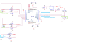
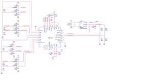
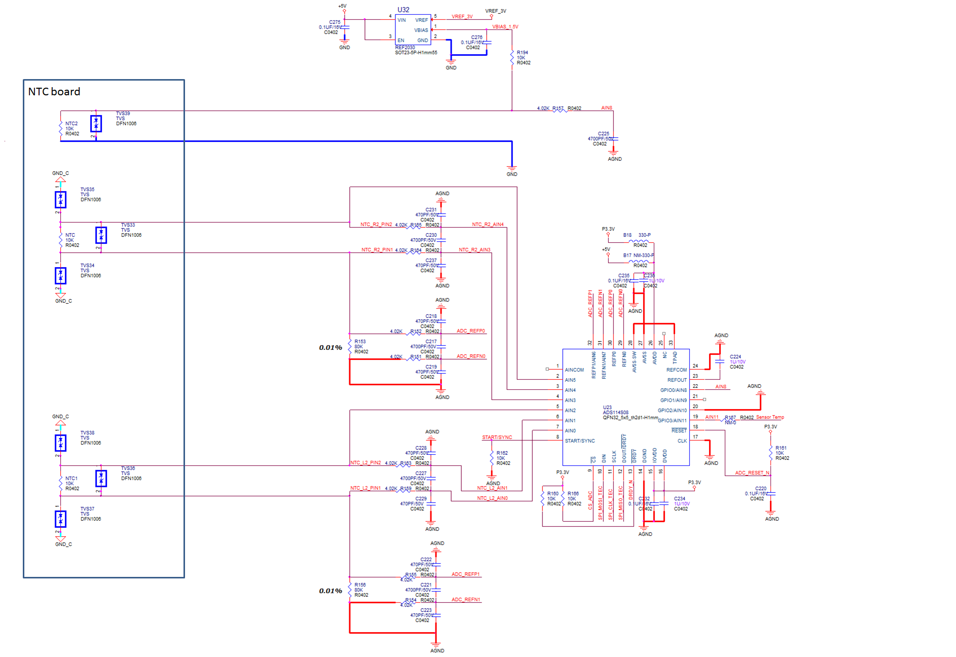
Could you help to review the two schematics below? Please only focus on analog inputs because other parts are not finished yet.

The schematics include both single-ended and ratiometric measurements.

For ratiometric measurement, one uses a common reference voltage (common Rref), and the other uses independent reference voltage and bias voltage like the design shown in ADS114S08 datasheet.

Can we further simplify the schematics to reduce passive circuitry for reference or bias voltage? 

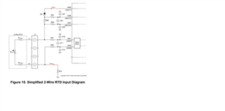
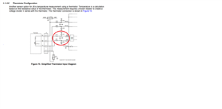
Can we get any NTC voltage if we correctly set input mux, reference mux and disable PGA?

For ratiometric, the voltage reference is from REFP/REFN pins and enable PGA

For single-ended, the voltage reference is from internal 2.5V and disable PGA

Thanks.

  • Do we need to put blocking diode D9 even if there is only one excitation current source used ? 

    I didn't see the diode used in other similar ADCs.

  • Hi Hector,

    The internal reference is used for establish the IDAC current and you are also using the internal reference for the single-ended measurements.  This requires a minimum cap value of 1uF between REFOUT and REFCOM, and REFCOM must also connect to AVSS (analog ground).  It is not clear the distance or possible interference that the single-ended inputs may encounter so it is recommended to at least use an RC antialiasing filter on the single-ended inputs.

    It is also recommended that the differential input filters use an antialiasing filter which would require a non-zero resistor be used in the filter path.  Also, it is recommended that the value of the differential input cap be at least 10x greater in value than the common-mode caps to prevent issues with drift.  For example, if C255 is 0.1uF, then C256 and C257 should be no greater than 0.01uF.

    The need for a diode may not be necessary.  The diode is meant to block reverse current into the ADC.  As long as the Absolute Maximum Ratings for the ADS114S08 are not exceeded, you should be fine limiting the values and use of passives.  However, if there is the possibility for transients from EMI/RFI to get into your system, then you may want to consider adding components or increased values of resistance so that the maximum ratings are not exceeded during the transient event.

    Best regards,

    Bob B

  • Hi Bob,

    Thanks for your feedback.

    The connection is shown in ADS1x4S08 EVK. 

    Does it use internal Vref so that REFP0 and REFN0 are not used actually? 

    Does it use differential measurement or it is still single-ended? 

    Is an RC antialiasing filter you mentioned shown in the red circle? 

    It is not clear the distance or possible interference that the single-ended inputs may encounter so it is recommended to at least use an RC antialiasing filter on the single-ended inputs.

    Thanks 

    Hector

  • Hi Hector,

    How and what reference input you use will depend on your method of excitation and circuit implementation.  Your initial schematic shows a current excitation.  To make the current excitation ratiometric you use the reference resistor as the reference input to cancel the IDAC drift out of the measurement.  The reference resistor must be at least as large as the largest thermistor resistance expected.

    In the picture you showed in your last post (from the EVM user's guide) you show a voltage excited measurement.  This uses the internal reference as the reference source.  The measurement is made ratiometric by exciting the thermistor from the internal reference output through a voltage divider.  So for this circuit the external reference input is not used.  The EVM has this connection as a part of the overall demonstration capability for the various different sensor types that can be connected.  In this circuit as drawn, the measurement is connected single-ended (referenced to ground).  This is just one way of implementing the circuit.  You could implement this differently on your board so that the voltage divider is swapped with the thermistor in the top position and the fixed resistor in the bottom position, but you would still want to measure the thermistor to keep the calculation as shown in the user's guide.

    And the input filter (antialiasing) filter is what you have circled.

    Best regards,

    Bob B

  • Hi Bob,

    For single-ended ADC measurement, can I use a simple RC filter (yellow)? 

    Do you suggest using filtering shown in the EVM user's guide (light blue)?

    Thanks 

    Hector

  • Hi Hector,

    For single-ended inputs you can use the less complicated method shown in the yellow outline.  The use of the differential input filter (the blue outline) would be appropriate for inputs where the input is not a single-ended connection.

    Best regards,

    Bob B

  • Hi Bob,

    I will use R/C value of the input filter used in ADS114S08 EVM on our board. I am selecting Rref and Rbias according to the calculation shown in the datasheet.
    It is not difficult to get Rref and Rbias from different IDAC and PGA gain. Do you have any suggestions to get the best performance by selecting appropriate IDAC and PGA gain? 

    Higher IDAC or lower is better?

    Higher PGA gain or lower is better?

    Higher PGA gain will amplify input noise as well?

    Thanks 

    Hector 

  • Hi Hector,

    You are correct in that there are tradeoffs for the various different scenarios.  Your choices will depend on your overall system and range of operation.  Usually the maximum IDAC current is dependent on the range of operation and the ability to overcome noise.  Higher IDAC current can help overcome some noise, but higher IDAC current can cause self-heating in the thermistor. 

    The maximum IDAC current that can be used will depend on the total resistance in the current path.  Here you will be limited by the compliance voltage as the total voltage drop across the path cannot exceed AVDD - 0.4V (for IDAC currents less than 1mA).  You will also be limited by the actual current steps for the IDAC current sources.  From the original schematic it looks like you are limited to 10uA, 50uA or 100uA.

    Also based on the schematic the NTC and reference resistor are the same so here you would be limited to a gain of 1.

    Here is an additional reference that might be helpful: A Basic Guide to RTD Measurements

    Even though the guide is specific to RTDs, many of the same concepts apply.  You may also find helpful C code for development from the Temperature Sensor Library Code.

    Best regards,

    Bob B

  • Hi Bob, 

    Here is a revised schematic using ADS114S08. The two-wire NTC low-side reference topology is used.

    NTC wire will be connected to the NTC board and then connected to a board (ADC chip is on the board) via cable. 

    The ground of the converter board is GND_C which is different from the other board.

    Use line to line and line to ground ESD protection by TVS.

    Please help to review the design. Any things we should concern about when we drive NTC by IDAC through cable.  

    Thanks.

    Hector

  • Hi Hector,

    It is not clear what TVS diode is being used or the clamping voltage.  Most of the I/O has a series resistance for limiting current through the ADS114S08 pins, however the pins used for IDAC current are not protected to limit any potential overvoltage current.  The Absolute Maximum Ratings for the analog pins is AVDD + 300mV to AVSS - 300mV with a maximum current of 10mA through the pin.  If the clamping voltage exceeds the analog supply range by more than 300mV, the ESD diodes will turn on and excessive current may flow through the pins.  The analog pins used for the IDAC current must must have the current limited to less than 10mA during the transient event.  It may be possible to add series resistors on these pins to limit current, but care must be taken to make sure that the IDAC compliance voltage is maintained for all the desired temperature measurement range.

    Also, there is inductance or ferrites on the analog supply.  This is not recommended as these devices can cause issues at startup and anytime needed current is required for device operation.

    Best regards,

    Bob B

  • Hi Bob,

    Thanks for your comments and review, I will add a 0402 footprint so that a resistor or diode can be soldered to protect the analog pins which are used for IDAC.

    Hector