A related question is a question created from another question. When the related question is created, it will be automatically linked to the original question.
If you have a related question, please click the "Ask a related question" button in the top right corner. The newly created question will be automatically linked to this question.
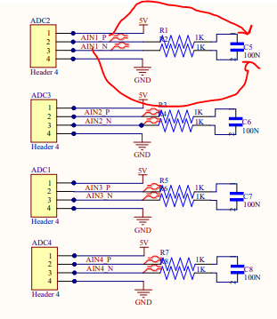
Note the reference design has placeholders for components that would add analog input filtering. I would suggest you do the same for your design and adjust the filter values as needed for the proper filtering response for your system.
As to the communication I think there is a misunderstanding. The ADS1234 uses an SPI compatible communication protocol and not I2C. If you intend to use I2C with the ADS1234 it will not work.
Thank you so much for your reply Bob. Now it makes sense. There seems to be an error in the datasheet then. Under 'Features' on the 1st page it says 'Two-wire serial interface'.
Since the naming convention on the pin did not specify MISO, MOSI, SCLK, CS the standard SPI terminology I had mistaken the protocol. (On the home page it says SPI.)
Thank you so much for your help. Regarding the pcb design, should I make the trace length for +- equal? Is this important for the accuracy of measurement. I can consider these traces as differential signals and match their length.
The trace length should be similar but it is not critical that the lengths are matched. The input is considered slow moving so high speed considerations are not a concern.
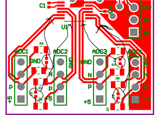
What would be more beneficial is having a solid ground under the analog signal traces. Your bottom layer has a solid block for +5V, but the signal traces run over the top of the +5V block and not ground. You might consider swapping the +5V and GND on the connectors so that the signal traces have an undisturbed ground all the way to the ADC.
Thank you for your suggestions. I have made the changes. Removed the resistors on the SPI bus, swapped 5V and GND, redefined the polygon and made the lengths match (more so for the visual appeal).
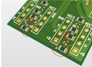
The layout is much better. I still think you should at least provide device footprints for an analog filter on the inputs, but that is up to you. If you have noise issues you will have to add them later.
I think the values chosen are a good starting point. As far as the implementation you are almost there. Currently your filter doesn't do anything, so move the net labels in your schematic to the other side next to the capacitor.
I would also suggest moving the capacitor closer to the analog inputs.
Also, make sure that the resistors stay within the ground area. So the resistors should be placed above the +5V power block.
There is one thing to consider with capacitor placement...for the capacitor to be most effective, the signal should flow through the capacitor before the signal connects to the ADS1234 input pins. It is true that the physical connection appears to be the same, but there is always some small resistance and inductance of the connection traces that effect the performance of the filter. So I would recommend moving 3 of the caps so that the cap is between the resistor and the ADC input pins similar to the connections from the ADC1 connector.