I've been using the ADS1256 for a while and so far I've inserted the t6 delay between every byte sent to or received from the ADS1256 just to be on the safe side and to simplify the logic. Now I'm considering to make the logic more efficient and use the t11 delays where applicable. However, I'm having a hard time to understand the t11 numbers in the figure 1 table in the datasheet.
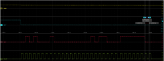
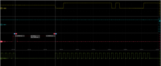
What does 4 T_CLKIN mean for RDATA? Is it the delay between any other command and RDATA or is it the delay between RDATA and any other command? In any case I need to wait t6 = 50 T_CLKIN before driving SCLK to read the sample data so I don't see the meaning of 4 T_CLKIN.
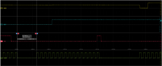
And what about WREG? Is t11 the time between the two bytes that constitute the command? Or between the bytes being written to the ADS1256 registers?
What about WAKEUP? That command is not even listed in the table.
By the way, it would be nice if you could provide a simulation model for the converter. Preferably in VHDL or Verilog.
/F