This thread has been locked.

If you have a related question, please click the "Ask a related question" button in the top right corner. The newly created question will be automatically linked to this question.

ADC128S052-Q1: Is the converted data (DOUT) from the current or previous address (DIN)?

Part Number: ADC128S052-Q1
Other Parts Discussed in Thread: ADC128S052

I assume since the 1st 3 SCLK cycles the ADC is in track mode and the fact that all the address bits get captured after the 5th SCLK cycles, the ADC is tracking the address bits from the previous 16-bit spi cycle regardless if it is in continuous mode (multiple conversions per spi frame) or normal mode (single conversion per spi frame).

But I am confused with below paragraph that was written in the datasheet.

"

There is no need to incorporate a power-up delay or dummy conversion as the ADC128S052 is able to acquire
the input signal to full resolution in the first conversion immediately following power up. The first conversion result
after power-up is that of IN0.

"

I would like to know what "power up" means in this paragraph.

1) Is it when the ADC actually powers up, Va and Vd?

    (so only useful one time after voltage rail powers up?)

2) Is it when Chip Select goes from high to low?

    (then how can you ever select the next address if the 1st conversion result after this kind of power up is always IN0?)

3) Is it when it transitions from the 16th cycle to the 17th cycle in continuous mode?

At the end, I would like to know if I can acquire all 8 channel data from only 8 conversions (16*8 SCLK cycles)?  Or would I need 9 conversions (16*9 SCLK cycles)?

And is there a minimum time for the Chip Select signal to be held high before re-asserting it low again?

  • Hello,

    Your understanding is correct, let me clear up what the paragraph is trying to say. Keep in mind this device was released almost 20 years ago, back then, devices would take longer to settle and have all the internal blocks powered up and ready to go, some devices suggested sending a "dummy" conversion and to throw away the data from the dummy conversion to initiate the device.  This device does not require that. The first frame will result in normal operation (selecting the mux input) and output the correct data. 

    1. power up means when Va and Vd and brought up from ground to the expected voltage. That first time that the Device is provided a voltage on the power supply pins. 

    2.No, power up here does not refer to any state of CS.

    3. No

    You will need 9 frames, there is a one frame delay to acquire the conversion data. Meaning in frame N, the user selects which channel to sample using the Address bits, and in the next frame, Frame N +1, the output measurement is clocked out. 

    Regards

    Cynthia

  • Hi Cynthia, thank you for the clarification.

    Can you also help answer my other question:

    "

    And is there a minimum time for the Chip Select signal to be held high before re-asserting it low again?

    "

    Also, so that means that I can actually get all 8 channel data from only 8 frames after power up right?

    And I would only need 8 frames thereafter for any subsequent requests right?

    Because the 1st frame after power up was pre-selected at channel 0 and will be converting channel 0.

    And I can have the 1st frame addressing channel 1 (while converting channel 0).

    : (etc.)

    And the 8th (last) frame addressing channel 0 (while converting channel 7).

    Another question, does the ADC chip register and keep holding the address obtained from the MOSI line indefinitely, regardless how long chip select is high for, as long as the ADC chip voltage rails don't power down?

    Thanks,

    ALbert

  • Sure, 

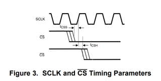
    There does not seem to be a minimum high time for CS stated, but common practice is a clock period. Also, there are time requirements relating SCLK and CS, these need to be met. let me explain the timing specifications, as this is a common question since the minimal is less than the typical. When the device released, there was different methods to specify requirements, which is no longer used. It is best to follow the typical values. 

    You are correct, if your application if find with starting with channel 0 and using the first frame to select ch1, then yes, you can use 8 frames to get all the channels. 

    Correct, as long as the device does not have a significant dip in voltage, the selected channel will be sampled in the following frame. 

    Regards,

    Cynthia