Other Parts Discussed in Thread: ADC128S052
I assume since the 1st 3 SCLK cycles the ADC is in track mode and the fact that all the address bits get captured after the 5th SCLK cycles, the ADC is tracking the address bits from the previous 16-bit spi cycle regardless if it is in continuous mode (multiple conversions per spi frame) or normal mode (single conversion per spi frame).
But I am confused with below paragraph that was written in the datasheet.
"
There is no need to incorporate a power-up delay or dummy conversion as the ADC128S052 is able to acquire
the input signal to full resolution in the first conversion immediately following power up. The first conversion result
after power-up is that of IN0.
"
I would like to know what "power up" means in this paragraph.
1) Is it when the ADC actually powers up, Va and Vd?
(so only useful one time after voltage rail powers up?)
2) Is it when Chip Select goes from high to low?
(then how can you ever select the next address if the 1st conversion result after this kind of power up is always IN0?)
3) Is it when it transitions from the 16th cycle to the 17th cycle in continuous mode?
At the end, I would like to know if I can acquire all 8 channel data from only 8 conversions (16*8 SCLK cycles)? Or would I need 9 conversions (16*9 SCLK cycles)?
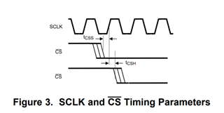
And is there a minimum time for the Chip Select signal to be held high before re-asserting it low again?