This thread has been locked.

If you have a related question, please click the "Ask a related question" button in the top right corner. The newly created question will be automatically linked to this question.

ADS1255: Driving the analog input.

Part Number: ADS1255
Other Parts Discussed in Thread: OPA2189, ADS1235, ADS1261

Hello, do you have an app note about driving the input stage on the ADS1255?  There is not really sufficient information in the datasheet.  It doesn't even specify the acquisition time as far as I can see.
For example, please see page 23 of this A/D converter.   This description is pretty comprehensive.
https://www.analog.com/media/en/technical-documentation/data-sheets/2400fa.pdf
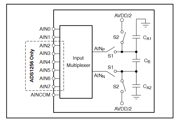
The ADS1255 shows an example of using 300 ohms and .1uF on the input (Figure 25) but makes absolutely no reference to how this effects settling time, etc.  Also, it makes no mention of how fast the amplifier needs to be that is driving it.

  • Hi Rick,

    Most of the information you are looking for is included  in the ADS1255 datasheet on pages 16 and 17. This includes the ADC input structure, the sampling time, and the effective impedance.

    How fast is your input signal changing? What BW do you need to measure? The ADC samples continuously at the modulator rate (called tSAMPLE in Table 9) so you will need to make sure your input signal is settled during this time.

    -Bryan

  • Hi Bryan,

    The pages you speak of discuss the input structure, but no spec is given for acquisition time, so I don't know that my input circuitry will allow the input to settle to 1LSB, or similar.  In the example datasheet I provided, there are two methods.  One is to keep the external capacitance very small and allow the input circuit to settle completely on each acquisition.  The other is to put a huge capacitor there and assume that the sample/hold caps in the A/D will charge from the huge external caps, and that the external cap will be large enough to charge the tiny caps in the A/D to 1LSB, or that it will at least average the input.  It sounds like the second option is what this datasheet proposes, but there is no reference to how stable this equivalent input impedance is over time and temperature.  There's a passing reference to 30ppm/degC for the reference input, but no relationship to the input impedance is implied.

  • Hi Rick,

    You will not be able to resolve 1 LSB of a 24-bit ADC, the inherent ADC (thermal) noise is too high. So you really want to target settling to the noise level of the data rate you choose (again, shown in Table 4 in the ADS1255 datasheet, assuming you will not use the buffer).

    There also isn't an acquisition time per se for a delta-sigma ADC. The input is sampled at the modulator frequency (fMOD) continuously during the conversion period. So you are not taking one sample during the "acquisition period", but many. On the ADS1255, this depends on the data rate. At a minimum, the ADS1255 takes 64 samples for the highest data rate (30kSPS). At 1kSPS, the ADC is averaging 30*64 = 1920 samples to provide one data output (see Table 11 and the Digital Filter description on page 11). The ADC is designed to settle within one modulator period assuming a very low input impedance source (this is similar to what is shown in the link you sent in your original thread). I would also not recommend a differential cap larger than 10nF as well, despite the drawing in Figure 25. The ADS1255 EVM uses 10nF caps between analog inputs.

    Do you have an idea what your source impedance will be? I don't think you will need to worry about settling time too much with the ADS1255 so you likely do not need a driver amp, but you might need a buffer depending if the source impedance is high.

    -Bryan

  • Right now I have designed the input to be driven from an OPA2189 configured as a single ended to differential driver.  That is, one amp is a buffer and the other is a gain of -1 inverter.  The input circuit is copied from the input of figure 25 of the ADS1255 datasheet, using the 301 ohm resistors and 100pF and .1uF caps... though you're telling me to use a .01uF cap instead of the .1uF.  This does make me nervous as there is no spec on how stable the input impedance is, and I feel I have to have a rock steady clock to maintain the input impedance, whatever it may drift to.  This is why I prefer a properly settling circuit so these things are not an issue, rather than rely on the average current being drawn.  Also, if I end up using the sync input to synchronize with other converters, won't that interrupt the modulator, allowing the external input capacitors to settle, and thus the input impedance will appear to change over time for each converter.  That is, during sync, modulator stops momentarily, then starts again.  External input caps settle when modulator stops, then begin drawing down again as modulator draws spikes of current.  If the modulator runs continuously, the current spikes would cause the voltage on the external caps to drop until an equilibrium is reached, but since I intend to sync it on an ongoing basis, this gives me much concern.

  • Hi Rick,

    The first thing that bears mentioning is that a delta-sigma ADC does not operate like a SAR ADC, so the same principles and methodologies cannot be applied to both. As I said in my last post, the ADC is guaranteed to settle within the level of the specified noise assuming a sufficiently low source impedance. Do you have a tentative value for the source impedance that your system will see?

    To drive this point home a bit more, you can see from the ADS1255 datasheet (Fig 7) that the mux resistance is 25ohm per channel. This feeds into a switched capacitor network (shown below), where the typical switch resistance is ~50ohm (not shown). The total resistance in this loop is then 2*(25 + 50) = ~150ohm. CB is given as 2.4pF when gain = 1, resulting in an RC network with a cutoff frequency of ~440 MHz (time constant = 2.3ns). Table 9 shows that the sample period for gain = 1 is 521ns, where the actual on-time is ~40% of that value, or 208ns. It takes ~18 time constants to reach 24-bit resolution, or about 41.4ns for the switch-cap network to settle within the 208ns allowable timeframe.

    (Note that this does not mean the resulting ADC noise is always resolvable to 1/2 LSB, just that the ADC is capable of settling to this level).

    With delta-sigma ADCs, settling issues typically result from a low-cutoff anti-aliasing filter at the ADC input where a very slow time constant does not allow the signal prior to being sampled. This is why you might want to avoid large caps across the ADC inputs, since they will take a lot longer to settle (depending on the filter resistors).

    It might also be helpful to understand what you want to do with the ADS1255. What kinds of signals will you measure? What is the source impedance? How quickly will the signals change? How fast do you want the ADC to sample? Again, a buffer might not even be required, and if not this will eliminate another source of noise, offset, and drift.

    -Bryan

  • Hi Bryan,

    I appreciate your patience dealing with this, as I've never found a comprehensive explanation for how the delta sigma converter works.  It's always generic and leaves me with questions that I think would be obvious.  For example, one explanation I saw recently had a counter counting up all the 1's in a conversion from the modulator, but if that's the case and given the time and frequency of the modulator, it can't count enough to get to 24 bits.  It's explanations like this that always have me scratching my head over exactly what is going on in there.

    Anyway, my application is to measure the output from a load cell, and also switch over to measuring the output from a high level analog output device.  I have the analog front end designed, complete with ESD protection, RF and other low pass filtering, gain, level shifting, and the switch that selects the appropriate input.  Below is a pic of what my analog input to my converter looks like at this time.  The input to pin 3 of U12 is a +/-2.5V signal from the previous conditioning, and the input labeled REF is a feed from the reference pin of the instrumentation amplifier, set at 2.5V.  The op amp is powered from +10V and -5V so I don't violate any common mode input voltage limits, and the input before this stage is clamped such that it cannot go above 5V or below 0V.  With said clamping, the outputs of this amplifier should never go above 5V or below 0V.  I haven't changed C63 to .01uF yet, as I'm trying to understand if that is even enough.  Also, if I sync this A/D to other channels on every conversion, will the modulator continue free running or will it stop/glitch momentarily.  My concern is that the caps on the input will average the input current, and if the modulator does anything other than continue running at normal speed, the average current will change and cause an error in measurement.  Likewise, since there is a voltage divider with the external resistors and the average input current, if the clock frequency changes at all, I think the average input current will also change and thus cause an error as well.  It has me wondering if having a cap across the input is a good idea at all.

    I know syncing on every conversion is much more aligned with how a SAR converter would be used, but I need to know that the converters will stay in sync, and be guaranteed that they will get back in sync if they were to ever get out of sync.  Lastly, my planned sample rate is 60Hz, so that I can reject any 60Hz signals that may be picked up by the cables connecting the load cell to the input.  Thanks.

    Rick

  • Hi Rick,

    Thanks for providing additional explanation.

    What is the output of the load cell? Is the load cell common-mode voltage at mid-supply (AVDD/2)? If so, load cell signals can often be measured directly by delta-sigma ADCs such as the ADS1235 or ADS1261. These ADCs are better suited for such measurements since they have integrated, low-noise PGAs that are also high impedance (like a true instrumentation amplifier). The ADS1255 PGA is different, and therefore only offers high input impedance with the buffer enabled, which also limits the absolute input voltage (though this might not be an issue depending on the bridge output voltage). You would then not need the buffer + inverting amp, since this only adds noise and error to your measurement.

    Can you explain what you mean by "sync this A/D to other channels on every conversion"? Do you have multiple devices running in parallel and you are trying to sync them to all start at once? What other channels are you referring to?

    The modulator will stop converting if you tell it to stop. The ADS1255 has a continuous conversion mode and a single-shot mode (see page 22). Single-shot mode takes a single conversion then stops (the modulator stops sampling), requiring user input to restart conversions. If you are going to be sampling repeatedly on the same channel, then use continuous conversion mode. If you are multiplexing through inputs (whether using the ADC mux or an external mux), you will at least have to manually restart conversions using the SYNC command or pin even if you are using continuous conversion mode. This lets the ADC know that it needs to flush out the digital filter so you don't get corrupted data i.e. data from the previous and current channels in the filter at the same time (see Figure 21).

    The external cap across the ADC inputs can be modeled as a resistor by taking 1/(2*pi*C*fMOD), where fMOD is the modulator frequency. For the ADS1255 at gain = 1, fMOD = fCLK/4 = 1.92MHz if fCLK = 7.68 MHz. A 10nF cap therefore looks like an 8.3ohm resistance. In parallel with the 150kohm ADC input impedance at gain = 1, this results in an error of 0.04%, or 427ppm. Increasing the cap may reduce this resistance and therefore the error, though this action then increases the external filter time constant, requiring longer time for an input step to settle. Like anything else, there is a tradeoff here, which is why I recommended 10nF as a good starting point. You could also look into the other ADCs I mentioned that have much higher input impedance. Or you can consider if the signals you need to measure are within the reduced input range with the ADS1255 buffer enabled.

    It might be helpful to share your schematic. If you do not want to post it in this open forum, you may request me as a friend by clicking on my name. We can then share information via private message if that is acceptable to you.

    -Bryan