This thread has been locked.

If you have a related question, please click the "Ask a related question" button in the top right corner. The newly created question will be automatically linked to this question.

DAC8775EVM: Boards spoiled after only a short time using it and SPI lines are not working properly after that.

Part Number: DAC8775EVM
Other Parts Discussed in Thread: DAC8775

Good day,

My organization has been testing on the DAC8775EVM due to the requirement of our project. I believe TI has produced a new DAC evm which is a more compact and smaller in size. The ones that we have is the bulkier and bigger one.

For a while, we have been testing the functionality of the boards by using the provided GUI and SPI lines communicating with an MCU to produce output.

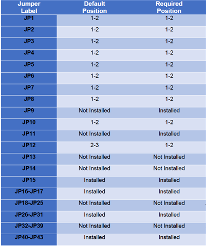
Below are the jumper settings that we are using on all the boards:

However, all of the boards are spoiled after some time and the GUI as well as the SPI lines are not able to function properly. The boards cannot be configured using SPI hence not able to get the correct output.

In the below excel file, shows a few observation and conclusion that we have on 3 of boards:

DAC8775_consolidated_HW-Observations.xlsx

The 4th board that we have, pins 2, 3 and 6 are shorted which are the SPI_CS, GND and SPI_DOUT. It seems  few of the SPI lines are shorted to ground. The other SPI lines are not shorted. I have checked the PVDD/AVDD, DVDD and VDUT test points and all are getting the correct voltage value.

Any opinions on this matter is appreciated as too many boards are spoiled after a short period of time. Thank you.

  • Hi,

    One my team member will look into the same and responds ASAP.

    Regards,

    AK

  • Dinie,


    First, what aspects of the device are you evaluating? It looks like you're making a lot of changes to supply sources. Most of the people that evaluate the device have just used the default setting and checked the operation of the DAC in current and voltage output modes. It's useful for looking at the output accuracy and checking the efficiency of the buck-boost.

    Going to your problem, there are a couple of things that might cause damage to the device. You can use external supplies to the device for the DAC outputs as shown in Figure 137 in the datasheet. However, enabling the buck-boost converter while attaching supplies to the VPOS_IN_x and VNEG_IN_x might be destructive to the device. Additionally, attaching an external supply to DVDD when the internal DVDD is enabled also might be destructive. I'm sure there are other ways that the device could be damaged depending on power connections, but those two are the first that came to mind.

    Do any of your external supplies have some current limiting? If you're swapping out supplies, limiting the current might help prevent something from burning out. I'm not entirely sure that would help. In your evaluations, I would start by using the EVM with the default setup. After that, you can just carefully change the supply configurations just to check on that operation.

    If you have more questions about the setup, please post back.


    Joseph Wu

  • Hi Joseph,

    As you have said, we are just measuring the output voltage and current by using SPI to internally configure the buck boost. The only external supply we gave is the 24V which is at J2 and VDUT at J1. No other external supply was given.

    All those connections we did was after the board was deemed not working properly. We did it to identify the issue.

  • Dinie,

    I did test the board with J9 and J11 installed and didn't see any problems. With J9 and J11 installed, the DVDD supply is sourced from the SM-USB-DIG and not the DVDD LDO on the device. I was able to set the device with both voltage set to the 0-5V range and current in the 4-20mA range. I have an external 24V supply that is connected to PVDD/AVDD through TP18. This should be the same connection as J2. 

    The Reference Out is enabled. The Power-off Condition is set to IOUT High-Z, VOUT High-Z and All Buck-Boost is set to All Enabled. 

    After that, you can set the Output Enable for the DAC and set the Mode (or range) and write to the DAC Data register and you should see the output at the output at J5 through J8 for the respective DACs. For these tests, I do have a 1kΩ load on each of the outputs for the current outputs.

    One thing that I think might be an issue is if you have the power applied to the board, and JP9 is installed while JP11 is uninstalled. In that condition, you may have the power from the SM-USB-DIG going into the DVDD LDO of the device while the LDO is enabled. This might damage the device LDO or the SM-USB-DIG (I haven't heard of damage happening, but I would imagine that it is possible.

    Joseph Wu