This thread has been locked.

If you have a related question, please click the "Ask a related question" button in the top right corner. The newly created question will be automatically linked to this question.

DAC11001A: slew rate

Part Number: DAC11001A
Other Parts Discussed in Thread: OPA828, , DAC11001B

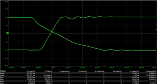
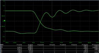
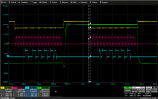
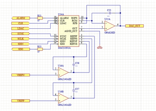
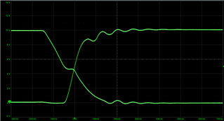
The slew rate seems to be dependent on slope direction, see screenshot. This is the DACs output buffered with an OPA828 (and another line driver). The initialization parameters are 0x02000200 and 0x06000080, after this 0x01FFFFF0 and 0x01000000 are repeatedly sent to the DAC to generate a full scale rectangular waveform. I tried also some other settings but that didn't help. What is the reason for this asymmetric behavior?

  • Hi Jurgen,

    What is the voltage output range of your DAC? What is the supply voltage of your OPA828? You can see slower settling time when the device is exiting overdrive, sometimes called overdrive recovery.

    Thanks,

    Paul

  • Hi Jurgen,

    Also, could you please share following information.

    1. Is that waveform has two separate DAC channels (one for positive slope and another for negative slope ) or  single channel both plot are merged.

    2. share your signal chain schematic  

    3. What is your SCLK frequency, share SPI scope snaps (two consecutive writes)

  • Hi Paul,

    the design is for +-10 V, DAC and op amp supply is +-15 V.

    Here is another screen, now with +-1 V on the output without changing anything on the hardware. Still different behavior for both slopes.

    Best Regards,
    Jürgen

  • Hi Anbu,

    the scope was set to trigger on both edges and set to persistent display - so only one DAC was involved.

    The SCLK frequency is set to 10 MHz, on the next screenshot you see green the output now toggling between -1 V and +1 V and the SPI signals as well.

    Here ist the DAC schematic, basically the green DSO trace is DAC_OUT with another buffer inbetween. I checked with a high impedance probe that there is no issue on that side. VREFP is +10 V, VREFN is -10 V. There is no C53 on the PCB.

    Best Regards,
    Jürgen

  • Hi Jurgen,

    Thanks for information , i will look and get back to you. 

    1. Could you please try the measurement with +10 V to 0V ,  change VREFP is 10 V, VREFN is 0V. 

    register setting and share snaps

    0x02000100 // Refer span 10V

    2. What is DAC supply voltage ?    AVDD = ? V , DVDD = ?V , IOVDD = ? , VSS = ? and VSS = ?


  • Hi Anbu,

    here is the screenshot with VREFN set to 0 and parameter changed to 0x02000100.

    AVDD = +5 V, DVDD = +3.3 V, IOVDD = +3.3 V, VCC = +15 V, VSS = -15 V

    Best Regards
    Jürgen

  • Hi Jurgen,

    I checked with my design team and behavior expected. It will not be symmetry. The  fall time is larger compare to rise time. 

    I would like to understand your application ?  any critical specification for slew rate.

    We have DAC11001B which is improved version of DAC11001A and can get symmetrical behavior for both rise and fall time.  

  • Hi Anbu,

    the current  application is nano-positioning but my board is more a generic design.

    I would really like to test the DAC11001B but there is no option to request samples on the web site and I couldn't find it at any of my distributors.

    Best Regards
    Jürgen

  • Hi Jurgen,

    This device is released couple of days back and it may take some time enable free sample.

    Wait for a week time and check. 

    I check with internal team to arrange samples if not enable in TI.com.

    Regards

    Anbu M

  • Thank you!