This thread has been locked.

If you have a related question, please click the "Ask a related question" button in the top right corner. The newly created question will be automatically linked to this question.

TSW1400EVM: Pattern File request

Part Number: TSW1400EVM

Hello!
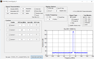
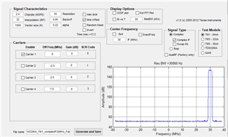
I need the pattern file to be used in TSW1400EVM.
There is WCDMA_TM1_complexIF30MHz_Fdata307.2MHz_1000.tsw as the provided pattern file, but WCDMA_TM1_complexIF30MHz_Fdata76.8MHz_1000.tsw with Fdata changed to 76.8MHz is required.

thank you.

  • Jong-min,

    Go to the TSW1400EVM product folder on the TI website and download the following software:

    Software for Creating High Speed DAC Patterns (Win 7 Version) – SLWC110.ZIP 

    See attached document for instructions on how to use these tools to create your requested test pattern.

    Regards,

    Jim

    slwu082.pdf

  • Hi Jim!

    Thanks for the reply.
    I know there are pattern generators too.
    However, there is no MATLAB license.
    Is there any problem in using the pattern generator without a MATLAB license?

    Thanks.

  • Not sure. Give it a try. If you have trouble, I can create this file for you. Just let me know what settings I should use on the attached slide.

    Pattern Gen.pptx

  • If there are no Matlab licensing issues, I think I can generate signals in the pattern generator.

    Which item of CDMA_EVDO/CommSignal/LTE/MCGSM/MultiTonePattern was created in the pattern below?

    C:\Program Files (x86)\Texas Instruments\High Speed Data Converter Pro\Test Files\WCDMA_TM1_complexIF30MHz_Fdata307.2MHz_1000.tsw

    thank you.

  • I think it was the program called "TSW1400_CommSignal_v1.exe" under the CommSignal folder.

  • Thanks for your reply and sorry for the late reply.

    I want to verify the contents confirmed in the TSW1400EVM and DAC3482EVM User's Guide in turn, and then check the results with the options I want.

    As shown in Figure 1, if you create a pattern (307.2MHz Fdata) and set the register, the Center Freq 90MHz signal comes out of the EVM board output.

    However, if you make a pattern (76.8MHz Fdata) as shown in Figure 2 and change the register 0 value from 0xF28C (Interpolation x4) to 0xF88C (Interpolation x16), no output comes out.

    Are there any registers that need to be modified additionally when the Fdata rate is lowered from 307.2MHz to 76.8MHz?

    DAC3482_FDAC_1228p8MHz_4xint_NCO_60MHz_QMCon.txt
       x00	   xF28C
       x01	   x0000
       x02	   x8052
       x03	   xA001
       x04	   x4DF1
       x05	   x0000
       x06	   x3400
       x07	   xFFFF
       x08	   x0000
       x09	   x8000
       x0A	   x0000
       x0B	   x0000
       x0C	   x05A6
       x0D	   x05A6
       x0E	   x05A6
       x0F	   x05A6
       x10	   x3000
       x11	   x0000
       x12	   x0000
       x13	   x0000
       x14	   x0000
       x15	   x0C80
       x16	   x0000
       x17	   x0640
       x18	   x205F
       x19	   x10F4
       x1A	   x4820
       x1B	   x0800
       x1C	   x0000
       x1D	   x0000
       x1E	   x1111
       x1F	   x8882
       x20	   x2400
       x22	   x1B1B
       x23	   x001F
       x24	   x1000
       x25	   x7A7A
       x26	   xB6B6
       x27	   xEAEA
       x28	   x4545
       x29	   x1A1A
       x2A	   x1616
       x2B	   xAAAA
       x2C	   xC6C6
       x2D	   x0004
       x2E	   x0000
       x2F	   x0000
       x30	   x61A8
       x7F	   x0001
    CDCE62005 Registers
    Freq:19.200000MHz
    Address	Data
    00		80400000
    01		813C0001
    02		81400002
    03		C10C0003
    04		00040004
    05		29F01A55
    06		44AF0006
    07		165294A7
    08		20001808

  • Jong-min,

    What is the DAC sample rate you are using? If it is 76.8MHz in the second case, the max NCO value can only be 1/2 of this rate. If you are still setting the NCO to 60MHz, lower this to something around 35MHz. If this doesn't help, send your GUI setting screen shots.

    Regards,

    Jim 

  • Hi Jim!

    The settings I want to use ultimately are:

    DAC sample rate: 1.2288GSPS
    Interface: 16-bit word wide
    Fdata rate: 76.8MHz
    Interpolation: 16x
    Bandwidth: 20MHz
    Fout: 500MHz
    PLL: Disable


    These are the clock and synchronization signals set on the actual board.

    DACCLK(P/N) : 1.2288GHz
    DATACLK(P/N) : 76.8MHz
    OSR(P/N) : 2.4MHz (?)
    PARITY(P/N) : None
    SYNC(P/N) : None
    FRAME(P/N) : None

  • Jong-min,

    For your setup I think OSR should be 4.8MHz. This is a divide by 256 for Y1 in the CDCE62005 Control tab. The FPGA clock should be divide by 16 (76.8MHz) for Y3.

    Regards,

    Jim

  • Hi Jim!

    In CDCE62005 of DAC3482EVM, OSR cannot be lowered to 4.8MHz.
    Does that mean that there is no way to check the Fdata Rate of 76.8MHz in DAC3482EVM?

    I will check it on the board made by our company.
    Thanks for the reply.

    Regards

  • Jong-min,

    Actually OTR can be 2.4MHz. 4.8MHz is the max but the equation for OSTR has that it can be divided down by any whole integer "n" per the data sheet. Are you using the DAC in dual sync source mode?

    Jim

  • Jong-min,

    I got this to work. Please try the example in the attached file.

    Regards,

    Jim

    DAC3484_16X_1228.8M.pptx

  • Hi Jim!

    Thank you so much for sending kind content.
    I set the same, but the output is not normal.

    The only difference is the DAC3484, DAC3482 and TSW1400 Source.
    TSW1400 Source Can you send the settings you made and the DAC3482EVM Register values?

    I'll attach my results.

    Regard.

    DAC3482_76.8MHz.pptx

  • Jong-min,

    There may be an issue with the imported file. Please use the multitone generator and create  a 20MHz tone and see if you can get a valid output from this following the instructions I sent. Once you get a valid output, we can focus on the pattern generator file you are trying to use. Follow the instructions I sent exactly as shown. Set the GUI to use the DAC3484, not the DAC3482. There might be an issue if you do not. Load the exact config file I call out which is in the DAC3484 folder.

    Regards,

    Jim  

  • Jim

    The result is not the same as yours.
    I'll attach the file.

    thank you for always quick reply

    Regard

    DAC3482_76.8MHz_2.pptx

  • In HSDC Pro GUI, set the tone selection to "complex", set the # of tones to "1" and select "DAC3484" for the device, not "DAC3482". 

  • Hi Jim

    As you said, I set it to DAC3484 in the HSDC Pro GUI and got the desired result as below. I have a few questions.

    1. I am using DAC3482, is there any problem with using the register value saved in DAC3484EVM?

    2. Not important, but is there any problem with setting DAC3482 in HSDC Pro GUI?

    3. In the board manufactured using DAC3482, dacclk_gone Alarm occurs. In the clock source, 1.2288GHz is exactly entered.

    (Even if you clear the dacclk alarm, it is not cleared.)  What should I check?

    Regard.

  • You can use the DAC3484 register values saved. I am testing with a DAC3482 myself. 

    For the dacclk_alarm, are you seeing this on the GUI somewhere? I cannot find this.

    Yes, you need to input 1228.8MHz to the board. Please verify your connections and jumper placement with the attached photo.

  • There is a little misunderstanding. The dacclk alarm did not come from the evm board, but from the board I made myself.

    Anyway, I set the above on the EVM board and checked the clock under normal output condition.
    dataclk was 153.6MHz and ostr was 9.6MHz. Is this correct?

    I think that if Fdata rate is 76.8MHz, dataclk is 38.4MHz, and ostr is 4.8MHz.

  • Please set FIFO Input Sync, FIFO Output Sync, Data Formatter Sync and Clock Divider Sync source to use the FRAME input signal, not OSTR. Your FPGA should send this signal along with the data and data clock to the DAC.

    Data rate is 76.8M, and the data clock should be 38.4MHz, not 153.6MHz, as this is a DDR interface, and the FRAME clock should be 

     fsync = fDATACLK/(n x 16) where n = 1, 2, …

    Regards,

    Jim

  • To synchronize with the Frame signal, can I control only the FRAME pin without using the Sync, Parity and Ostr pins?

    I am sending dataclk (38.4 MHz) and Frame (2.4 MHz) from the board I made to the DAC from the FPGA, but nothing comes out.

    Can you check the DAC Register? (with Read-only)

    Regard.

    dac3482_reg.txt
    0x00=0xf884
    0x01=0x0100
    0x02=0x8082
    0x03=0xa001
    0x04=0xffff
    0x05=0x0460
    0x06=0x3900
    0x07=0xffff
    0x08=0x0000
    0x09=0x8000
    0x0a=0x0000
    0x0b=0x0000
    0x0c=0x0400
    0x0d=0x0400
    0x0e=0x0400
    0x0f=0x0400
    0x10=0x0000
    0x11=0x0000
    0x12=0x0000
    0x13=0x0000
    0x14=0x3333
    0x15=0x3333
    0x16=0x3333
    0x17=0x3333
    0x18=0x205f
    0x19=0x10f0
    0x1a=0x8820
    0x1b=0x0800
    0x1c=0x0000
    0x1d=0x0000
    0x1e=0x1111
    0x1f=0x8882
    0x20=0x2201
    0x21=0x0000
    0x22=0x1b1b
    0x23=0x001f
    0x24=0x1000
    0x25=0x787a
    0x26=0xb6b6
    0x27=0xeaa8
    0x28=0x4541
    0x29=0x1a1a
    0x2a=0x1616
    0x2b=0xaaa2
    0x2c=0xc4c4
    0x2d=0x0004
    0x2e=0x0000
    0x2f=0x0000
    0x30=0x6020
    0x7f=0x540c

  • Jong,

    You do not need Sync, parity or Ostr to get an output.

    You have a couple register settings that are incorrect. Please see attached file. One critical one

    dac3482_reg new.txt
    0x00=0x0884  //new
    0x01=0x0001  //new
    0x02=0x8082
    0x03=0xa001  
    0x04=0xffff
    0x05=0x0460
    0x06=0x3900
    0x07=0xffff
    0x08=0x0000
    0x09=0x8000
    0x0a=0x0000
    0x0b=0x0000
    0x0c=0x0400
    0x0d=0x0400
    0x0e=0x0400
    0x0f=0x0400
    0x10=0x3000  //new
    0x11=0x0000
    0x12=0x0000
    0x13=0x0000
    0x14=0x3333
    0x15=0x3333
    0x16=0x3333
    0x17=0x3333
    0x18=0x205f
    0x19=0x10f0
    0x1a=0x8820
    0x1b=0x0800
    0x1c=0x0000
    0x1d=0x0000
    0x1e=0x1111
    0x1f=0x8882
    0x20=0x2201
    0x21=0x0000
    0x22=0x1b1b
    0x23=0x001f
    0x24=0x1000
    0x25=0x787a
    0x26=0xb6b6
    0x27=0xeaa8
    0x28=0x4541
    0x29=0x1a1a
    0x2a=0x1616
    0x2b=0xaaa2
    0x2c=0xc4c4
    0x2d=0x0004
    0x2e=0x0000
    0x2f=0x0000
    0x30=0x6020
    0x7f=0x540c
    was address 0x10. The data sheet mentions you must set bits 13 and 12 to "1" for proper operation of part. The default values are "0" for some unknow reason to me. I could see how a user could miss this. I tried this file on my setup and everything works fine.  

    Regards,

    Jim

  • Jim!

    I set the modified register value, but there is no output.

    I think the problem is that register 0x05 (Bit 10) alarm_dacclk_gone goes high. Even if register 0x05 is reset, alarm_dacclk_gone is still high.

    What do you think is causing alarm_dacclk_gone to be high?

    Regard

  • Jong,

    It appears the DAC is not getting a clock from the CDCE62005. Make sure you have an input clock at J9.Make sure Y2 is enabled on the CDCE62005 Control tab. I would suggest probing R15 to verify the clock is present. This resistor should be near the clock input pins of the DAC.

    You can also go the CDCE62005 Control tab, enable Y4, set the divider, and verify there is a clock at SMA J10. 

    If all looks fine, go back to your orignal config file and see if you still get this alarm.

    Regards,

    Jim

  • Hi Jim

    It took me a while to fix the dacclk_gone issue.

    If I set the data rate to 76.8MHz, in Figure 51, 'SAMPLE0' is 76.8MHz Rate, and I0 and Q0 are also 76.8MHz Rate, so D[15:0]P/N is 153.6MHz right?

    Regard,

  • Jong-min,

    The DATACLK is 1/2 the data rate. So if your D[15:0] inputs are switching at 153.6MHz, your DATACLK should be at 76.8Msps.

    Regards,

    Jim 

  • Jim

    In order to use the sample rate of 1.2288GSPS using interpolation 16x, as in the last picture, should the D[15:0] input be set to 153.6MHz? Or should I set D[15:0] to 76.8MHz?

    Regard

  • The DATACLK should be running at 76.8MHz which will result in the DDR data rate to be 153.6MHz.

  • Jim.

    It is the same as the environment tested on the EVM board, but the result is not understandable.

    A file containing the results is attached. What do you think?

    Regard.

    DAC3482_76.8MHz_fDAC1.2288GHz.pptx

  • Jong-min,

    Set address 0x20 to 0x2201. Currently you have this address set to 0x0000.

    Regards,

    Jim

  • Jim.

    It is the same even if 0x20 is set to 0x2201.
    Thanks for the quick reply.

    Regard.

  • Your test results showed several different interpolation plots. Which one is required for your application and what is the issue? I could not tell by the data.

    In your testing, when you changed the interpolation factor, did you also change the DATACLK or the data rate?

  • fDATA is 76.8MHz and fDAC is fixed at 1.2288GHz, and the clock does not change when interpolation changes. We simply changed bit[11:8] in Register 0x00.

    If the Register value changes, what should I do to apply it? For example, to activate the update register.

  • Jong-min,

    DAC data rate = DAC sample clock / Interpolation. If you change the interpolation value, you must either change the DAC sample rate or the DAC data rate.

    Regards,

    Jim  

  • jim

    I confuse you by sending multiple interpolation outputs.
    As I checked on the EVM board, I wish there was only one output signal at Fc 19.2MHz. However, as you can see, there are 7 of them at 19.2MHz intervals.

    When setting the register value in the dac3482, should the register setting be different when starting and in progress?

    regard

  • Following the procedure I sent, I do not see the spurs you are getting (see attached). Please make sure to always run the GUI as system administrator. Otherwise, some problems may occur.

    19.2MHZ_tone_1228.8MHZ_Fs_16x_int.WMF

  • Jim

    There is no problem when testing with EVM board. Of course, I also run the GUI as a system administrator.

    I have a few questions.

    When testing with the EVM board, I tested it with the DAC3484.
    Register value was set and applied as DAC3484 in TSW1400EVM.

    1. DAC3482 is applied to the board I actually designed.
    Is it okay to apply the register value set in DAC3484 to DAC3482 as it is?

    2. Can't you check the output by setting DAC3482 on the EVM board?

    Regard

  • Jong-min,

    It appears there is an issue with the GUI doing all of the writes from a config file. I was seeing the same spurs as you were when I load the config file. If I issue any command on the GUI after loading the config file, or do one extra read command to the config file, the data gets loaded properly and the spurs go away. Try the attached config file which has an extra read command added. This was tested with a DAC3482EVM and the output was fine.

    Regards,

    Jim

    DAC3482_FDAC_1228p8MHz_16xint.txt
       x00	   xF884
       x01	   x0100
       x02	   x8002
       x03	   xA001
       x04	   x7DF1
       x05	   x0460
       x06	   x2A00
       x07	   xFFFF
       x08	   x0000
       x09	   x8000
       x0A	   x0000
       x0B	   x0000
       x0C	   x0400
       x0D	   x0400
       x0E	   x0400
       x0F	   x0400
       x10	   x0000
       x11	   x0000
       x12	   x0000
       x13	   x0000
       x14	   x0000
       x15	   x0640
       x16	   x0000
       x17	   x0640
       x18	   x205F
       x19	   x10F0
       x1A	   x8820
       x1B	   x0800
       x1C	   x0000
       x1D	   x0000
       x1E	   x1111
       x1F	   x8882
       x20	   x2201
       x22	   x1B1B
       x23	   x001F
       x24	   x1000
       x25	   x787A
       x26	   xB6B6
       x27	   xEAA8
       x28	   x4541
       x29	   x1A1A
       x2A	   x1616
       x2B	   xAAA2
       x2C	   xC4C4
       x2D	   x0004
       x2E	   x0000
       x2F	   x0000
       x30	   x6020
       x7F	   x0004
       x06     x2A00
    CDCE62005 Registers
    Freq:0.000000MHz
    Address	Data
    00		80400000
    01		813C0001
    02		81400002
    03		C11C0003
    04		00040004
    05		29F01A55
    06		44AF0006
    07		165294A7
    08		20001808
     

  • Jim

    Are the config values of addresses 0x1E and 0x1F equal to 0x1111 and 0x8882?
    It seems to need modification to use Frame Sync.

    Regard

  • Jong-min,

    These values are correct. I was not using the NCO or mixer so the upper bytes are do not care. Address 0x1E has no option for Frame Sync.

    Address 0x1F must have bit 4 set to "1" and bits 3:2 set to "0" for Frame sync and this is true with a 0x8882.

    The other register that controls Frame Sync ix 0x20.

    Regards,

    Jim

  • jim

    For bit4 to be '1', it must be '1', not '8'.
    bit15~bit12/bit11~bit8/bit7~bit4/bit3~bit0

    Regard

  • My mistake. You are correct. But bit 4 is for the NCO SYNC select, and I was not using the NCO, so this setting does not matter unless you plan to use the NCO.

  • If you are using NCO, is it correct to apply 0x8812 to 0x1F?

  • Not 100% sure since the mixer does not have an option for FRAME sync. With this setting, you would have to manual toggle SIF SYNC for the mixer SYNC source. 

  • Hi Jim

    In DAC3482, if you want to set a register, you need to do a RESET and then it seems to be applied.

    Anyway, I modified the register settings, data and clock to get the desired result.
    Thanks for your help for a long time.

    Regard