This thread has been locked.

If you have a related question, please click the "Ask a related question" button in the top right corner. The newly created question will be automatically linked to this question.

ADS54J60: Inquriy about ADC input reference design

Part Number: ADS54J60
Other Parts Discussed in Thread: TSW54J60EVM

Hello,

My customer is considering using the ADS54J60 to analyze about +/- 500mVp-p differential DC input signal as below.


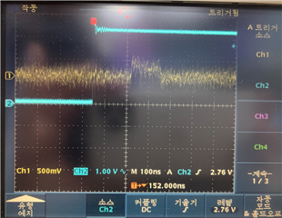
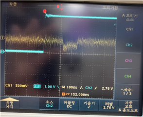
Positive & Negative dc input capture image(Yellow signal)

They believe that the ADS54J60 cannot receive the signal directly because the common-mode voltage levels are different. Is this correct?

Can you please suggest an ADC input reference design so that they can receive the above signal using the ADS54J60?

Thank you.

JH

  • JH,

    They will need an amplifier for this to work. Have them look at the TSW54J60EVM, which has two amplifiers feeding the two inputs of one ADS54J60. This board and design files can be found under the TSW54J60EVM product folder on the TI website. I would also post this to the high speed amplifier forum for more suggestions.

    Regards,

    Jim