- Ask a related questionWhat is a related question?A related question is a question created from another question. When the related question is created, it will be automatically linked to the original question.
This thread has been locked.
If you have a related question, please click the "Ask a related question" button in the top right corner. The newly created question will be automatically linked to this question.
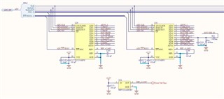
We are witnessing large non-linearities in the conversion output data. Using precision controlled voltage sources (inputs channel 0 and 1 for this test) I am able to see large jumps in output count value corresponding to what should be an LSB change. I am suspicious of the the 4 LSB bits as I often see a +/-16 bit jump in the output conversion data. I am giving the conversion plenty of time as I don't read out the data until ~100ms after EOC goes high. I have tried configuring CFGR2 only at powerup and also interleaving configuration between conversions and still see the conversion errors. Schematic pasted below for reference. Please advise.
Operating Mode: 3.3V supply, 16-bit output length, MSB first, Unipolar, external 2.048V reference, EOC, Normal Mode.
Hi Curtis!
Welcome to our e2e forum and I'm sorry to hear that you are having issues with the TLV2556! Can you try an experiment for me? See if you can tell any difference in the conversion results if you sample CH0 twice in a row then CH1 twice. Compare the first and second conversion result for each channel and let me know if you see any difference. In your schematic, I see a resistive divider on CH6 - is there anything off page that would be buffering the inputs to the TLV2556?
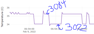
Hi Tom. I changed the code to continuously sample CH0 and the issue remained. See plot below showing ADC count value jump between 3072 and 3084 with no conversions at values in between even though I am ramping a precision voltage source between these input values (ignore axis units).
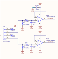
See buffer schematic below showing AD590 temp sensor circuit driving AIN0s of the converters.
Hi Curtis,
Thank you for the added detail! Your amplifier only has ~400k of bandwidth and its driving into ~1.8nF of capacitance internal to the TLV2556. Can you grab a screen shot from an O-Scope right at the AIN0 input to the ADC? You may be experiencing some large over/under shoots causing your conversion problems.
How fast is the I/O Clock? I can't really make out any detail of your 3072 vs. 3084 result without the /CS, and I/O Clock, so if you can include those signals and send another capture, that would be great.
Tom, the plot shown above is not showing SPI interface signals, it's a plot of the 12bit conversion data output being sampled at a 10Hz rate. SPI SCLK is 6MHz.
Still need to see the actual signals on the SPI lines though Curtis. O-Scope preferred to logic analyzer.
Don't have good probe points for TLV2556 chip. Holding 2 scope probes on IC pins, long ground connection so this is not an ideal setup but good enough to capture SPI signals. Setup sampling on loop and triggered on rising edge of CLOCK to capture transactions.
Multiple transactions DATA OUT (yellow), CLOCK (green)
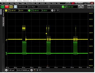
Single transaction DATA OUT(yellow), CLOCK (green)
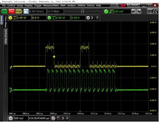
Multiple transaction CS (yellow), CLOCK (green)
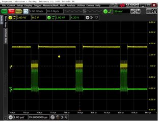
Single transaction CS (yellow), CLOCK (green)
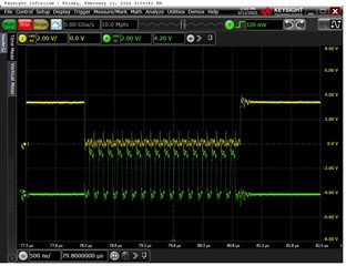
Thanks for the scope shots Curtis,
Hard to tell, but the first multi sequence seems like a full scale input, your 0xC0C, and then maybe 0x001 or 0x002. The second one is clearly 0xC0C (7084) that you mentioned before. Was your input held constant, still only sampling CH0? Were you able to capture the input directly on the analog input (after your buffer)? You could do that while triggering on the /CS line.
In the first screen shot, you seem to have ~15uS between conversion, while the last one with CS, it looks like a little over 3uS. Are you constantly changing the overall sample rate? Initially you said you were sampling at 10Hz.
Let me clarify the current sampling scenario. I am sampling all the ADC channels once per second, I cycle through all the channels (0h to Dh) with approx ~15uS between individual channel conversions. I just grabbed one of the transactions to show in the plots and because I am also sampling the TEST inputs I would see a full scale output (Dh). Input CH0 was held constant during this test and I would need to setup an active probe to get results worth viewing on the scope for the opamp output. What are your concerns if the input is held constant?
Curtis -
It's easier to debug something if you hold things relatively constant, sample rate and Vin are examples. The TLV2556 samples a new input while it converts the last one. If you sample at 10Hz, you run the risk of faulty conversion results due to leakage on the sample and hold capacitor. If you continually sample the same channel with the same input voltage, you can see sample-to-sample variations that might be considered as non-linearity or LSB errors. If you slow your clock down, you actually increase your sample time which would be beneficial to you potentially with the 400kHz BW driver you are using. Having an RC between the driver and AINx would also be a potential solution to your LSB issues.
I don't follow your leakage comment as the datasheet describes the conversion process as being controlled by the internal oscillator and kicks off directly following the sample stage. It shouldn't matter if I wait ten minutes between conversions. Following the last clock of an SPI transaction it switches from sample to conversion and once conversion is complete the result is latched to be read on the next SPI transaction. Please elaborate on the risk of faulty conversions due to leakage.
Hi Curtis,
Sorry - I was thinking of a different device. You are correct, the internal conversion clock of the TLV2556 should relax sample rates. Let me know when you have a chance to look at the analog input sampling instance.