This thread has been locked.

If you have a related question, please click the "Ask a related question" button in the top right corner. The newly created question will be automatically linked to this question.

ADS1220: Measuring AC peak in HV induction

Part Number: ADS1220
Other Parts Discussed in Thread: REF2041,

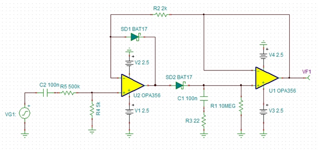
We are measuring an induced AC voltage (50/60Hz) that can range from 100mV PP to 150V.  Isolation would be nice but that can come later.  We were looking at a peak detector with AC coupling into a 100:1 voltage divider and then to the peak detector.  Similar to this:

 Thanks Kai for the head start.

R2 provides feedback to the buffered output that includes the diode forward drops. What determines its optimum value?

ADC will be the ADS1220.  The opamp power will be rail split for a single 5V supply.

  • Charles,

    The attachment is not viewable.  Can you please re-attach? I will help you optimize your circuit.

    Best regards,

    Art

  •  I believe R2 is just a current limit for SD1 and has no specific design value. i.e no gain function.

    My final circuit turns this into a peak detector. Turned it into a single supply by using the REF2041 as the 2.048V amplifier mid point reference and then sending the 4.096V to the ADS1220 REFP0 input.  This way I can use the ADS1220 differential AN2-3 input with internal 2.048 reference or go full 0-4.096 single ended with the system 0VAC input producing a 2.048 output to the ADC.

    What is slightly confusing about the ADS1220 is figuring out the usable common mode range.

    Peak Detector OPA397.TSC

  • Charles,

    Some background on the amplifier circuit:  R2 is feeding back the "peak detected" voltage for comparison to new input signals from Vg1.  For your information, here is a link to document on a "half wave rectifier circuit" that is the core of your circuit. https://www.ti.com/lit/an/sboa227a/sboa227a.pdf  The main component that converts the half wave rectifier to the peak detector is C1.  R1 is used to "reset" the detector slowly.  R3 keeps the circuit stable.  U1 buffers the sampled signal so that the capacitor C1 is not reset by other impedances (e.g. the ADC input impedance).

    Regarding your direct question:  The common mode depends on whether you are using the PGA or not.  If you are using the full +/-2.5V amplifier range, you will probably want to use the ADS1220 in "pga bypass mode" in this mode you have a common mode range of AVSS-0.1V to AVDD+0.1V.  The differential input range is -Vref/Gain to +Vref/Gain.  Even though it is called "PGA bypass" you do have a gain selection of 1 to 4.  If you need higher gains you will have to use the PGA and the common mode becomes more complicated, but I doubt you need this.  Note that the PGA is a linear amplifier and in bypass mode the input uses a switched capacitor divider circuit on the input.  for large input impedances sometimes it is advisable to use the PGA even in low gains, but you already have an amplifier buffer so the PGA is not needed.  You could test this all with the ads1220evm: https://www.ti.com/tool/ADS1220EVM

    I hope this helps.  Let me know if you have further questions.