


Part Number: TSW1400EVM
Hello,
I am trying to test an ADC3243EVM with a TSW1400 board. After loading ADC324x_2W_14bit firmware and launching a capture, I'm getting "Clock from ADC EVM not received by FPGA board" message from HSDC Pro software.
Indeed, all LEDs of the TSW1400 are ON except USER_LED3 and USER_LED4.
I supply the TSW1400EVM (on port J12) by using a 5V 4A bench power supply, and ADC3243EVM (on port J15) with a 5V 3A power brick.
ADC3243EVM jumper connections are :
* JP1 -> 2,3
* JP2, JP3, JP4, JP5 -> closed
* JP6, JP7 -> 1,2
TSW1400 jumper connections are :
* JP3, JP4, JP8 -> 2,3
* JP5, JP6, JP7 -> closed
A 40 MHz, 0 dBm clock from a RF signal generator is provided to the ADC3243EVM port J9 (CLK). J1 (CHA) and J4 (CHB) ports are not connected.
The ADC3000 GUI isn't installed on my computer, I only use ADC3243EVM SW1 to reset the ADC3243 registers to default.
I already have checked the supply voltages of the 2 boards -> they seem fine.
I also measured DCLK and FCLK at the ADC3243EVM HSMC connector with differential probes. FCLK looks clean and locked at 20 MHz (fig 1). DCLK is also locked at 140 MHz, but seems less clean (fig 2).
Can someone tell me where my problem could come from ?
Thanks,
Aymeric
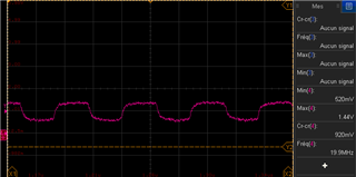
fig 1 : FCLK
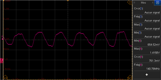
fig 2 : DCLK

