This thread has been locked.

If you have a related question, please click the "Ask a related question" button in the top right corner. The newly created question will be automatically linked to this question.

TSW14J57EVM: timed_out_error

Part Number: TSW14J57EVM
Other Parts Discussed in Thread: ADC08DJ5200RFEVM

Hi Team,

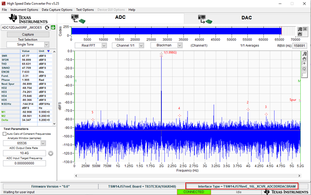
The customer is using a TSW14J57EVM with ADC08DJ5200RFEVM. Unfortunately they can not capture anything with HSDC Pro, software, since they get a TIMED_OUT_ERROR.

The customer followed all the steps in the User Guides however, the problem still persists. The LED D3 is off and the LED D4 is not blinking, does this mean that the FPGA does not recognize the ADC?

Here is the the steps that the customer did:

- Connect FMC+ connector between boards

- Connect +12V power to TSW14J57EVM

- Turn on +12V power supply (>3 A) and move power switch to ON position

- Connect +12 power to ADC08DJ5200RFEVM (> 2 A) 

- Connect USB3.0 cable between TSW14J57EVM and PC

- Connect USB2.0 cable between ADC08DJ5200RFEVM and PC

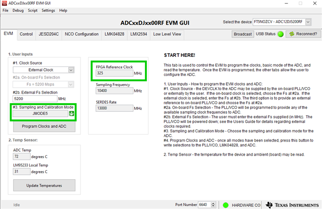
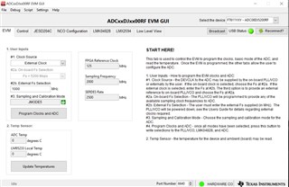
- Launch ADCxxDJxx00RF EVM GUI

- On User Inputs, select " Clock Source" = "On-board", "On-board Fs Selection" = "5200 Msps",  "Sampling and Calibration mode" = "JMODE5", click "Program Clocks and ADC button". 
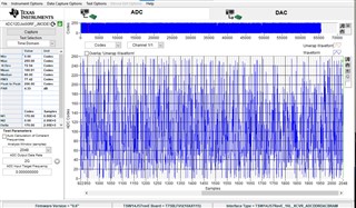
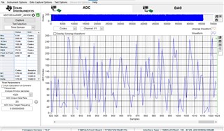
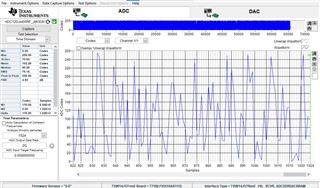
- Launch HSDC Pro

- The board is detected, and I click OK

- No firmware popup is displayed, click OK

- Using Select ADC pulldown choose “ADC12DJxx00RF_JMODE5” , then click OK

- In ADC Output Data Rate field type “10.4G” and press Enter on keyboard.

- Click Capture button at upper left of GUI.

At this point they get this error message:

Read DDR to file TIMED_OUT_ERROR 

at this point, the LED D1, D3, D8, D9 are ON. D2, D4, D7 are OFF. D5 and D6 are slightly ON (the light intensity is lower  than the others LEDS which are ON). 

Could this be caused by using a wrong firmware file and not working with this ADC?

What could you recommend to solve this issue?

Thanks in advance,

Regards,

Marvin

  • Hi Marvin,

    The EVM is setup to use external clock option by default. If you need to use the onboard clocking please follow instruction in users guide. Here is the screen shot of the changes. Or you use follow the instruction for external clock and provide external clock. 

  • Hi Neeraj,

    Thank you for the response. Here is an update from the customer:

    The customer mentioned using the On-Board Clock Configuration, but with an External Clock Configuration, and got the same time out error and the same LEDs on/off.

    However, instead of the firmware “ADC12DJxx00RF_JMODE5” mentioned previously, they tried the Firmware "TSW14J57revE_DDR_RxOnly_L8_Reconfig_FIRMWARE.rbf" for the FPGA from the HSDC Pro GUI, selecting "Instrument Options > Download Firmware" , then going in the folder "C:\Program Files (x86)\Texas Instruments\High Speed Data Converter Pro\14J57revE Details\Firmware".

    When the firmware is downloaded to the FPGA, the LEDS acts differenly than before:
    D1 off
    D2 blinking
    D3 off
    D4 on
    D5 slightly on
    D6 off
    D7 off
    D8 on
    D9 on


    Looks like at least with this firmware the ADC established a SYNC with the FPGA (LED 3 off), but the FPGA can not detect the device clock from ADC since LED4 is not blinking

    Can you confirm if the customer is using the wrong firmware? or is there anything that they missed when selecting the On-Board Clock configuration?

    Another thing is that the customer is not using the Bandpass filters as specified in the User Guide: could this be the problem why the device clock from ADC is not detected by the FPGA?

    Thanks again for the support.

    Regards,

    Marvin

  • Hi Marvin,

    There are couple of things that could be wrong. 

    1. if using the external clock option and clock of 5.2GHz in JMODE5 the ref clock for the FPGA should be 325MHz. Here is the screenshot of the gui. 

    2. Please use the TSW14J57RevE_16L_XCVR_ADCDDRDACBRAM firmware. This is default firmware which gets loaded when ADC12DJxx00RF_JMODE5 file is loaded. 

    3. Make sure the jumper labeled REFSEL(J13) is installed when using external clock option. 

    Regards,

    Neeraj 

  • Hi Neeraj,

    Thank you for the help. Here is the response from the customer:

    "I discovered that the waveform generator that we were using was broken, hence we did not get a correct sampling clock. Now we are using a correct one. But I still have some problems. I think could be related to the Firmware provided and I will try to explain why.
    So this is what I do:
    - Connect the FMC+, connect the power cables and power on the board, connect the USB cables.
    - Open the "ADCxxDJxx00RF EVM GUI", select "External clock", select "1000 MHz" (because I provide a 1GHz sampling clock with a pulse generator), select "JMODE5", click on "Program Clocks and ADC". See picture "ADC_GUI". Please note that I am providing externally a sampling clock of 1GHz, a reference clock of 125 MHz, and a square waveform to be sampled and detected by the ADC. And yes, jumper J13 is installed.
    - Open "HSDC Pro", and now I should choose the device from the drop-down list above the "Capture" button.

    Now my first question: in the list provided, there is nothing directly related to the ADC that I am using, which is the ADC08DJ5200RFEVM. I think I should find in the list something like "ADC08DJxx00RF_JMODE5" but it does not exist. Does it exist something specifically for my board, or is it ok to select another device from the list which will work anyway with my board (for example the "ADC12DJxx00RF_JMODE5")?
    Meanwhile, I tried with the "ADC12DJxx00RF_JMODE5":
    - I select this device in the drop-down list, then at the question "Do you want to update the firmware for the ADC?" I click "Yes". I get LEDs 1,3,5,6,8,9 ON and LEDs 2,4,7 OFF. I click on Capture and I capture something (so I don't have the TMED_OUT_ERROR anymore) but I only see noise. You can see it in the "picture1" attached.

    Here my second question: how is it possible that , even if LED3 is ON (means that ADC and FPGA not SYNC) and LED 4 is not blinking (means that clock of ADC is not sampled by FPGA) we don't get a TIMED_OUT_ERROR as before?
    And then my third questions, why we are only sampling noise and not the input waveform that I am sending with the waveform generator (I am sending a square wave)?
    And if I try to Capture again (by clicking on the circled arrow "Click to reload device INI" and then clicking on "Capture"), I get the exact same noise waveform as before, you can see the attached "picture2" and "picture3" which are two different Captures, but they are exactly the same waveform. Here my fourth question: how is that possible? Should't they be two different waveforms since I am sampling in two different time instants?

    Picture 1

    Picture 1

    Picture 2

    Picture 3

    GUI

    Thanks in advance for the help, I tried to explain everything as precise as possible in order to have no misunderstandings."

    I hope this helps.

    Regards,

    Marvin

  • Hi Neeraj,

    Any update on this follow up question?

    Regards,

    Marvin

  • Hi Marvin,

    The plots you send does not look like valid data. This looks like junk data. 

    Can you please try following. 

    1. Make sure the DEV CLK and FPGA ref clk are sources are in synchronized with each other with 10M ref. 

    2. The INI file named ADC12DJxx00RF_JMODE5 is the correct file you use. 

    Regards,

    Neeraj

  • Hi Neeraj,

    Thanks for the help. Here is the response from the customer:

    "I think that the DEV and SYS REF clocks are phase locked since they come from the same pattern generator.

    And I am indeed using the INI file ADC12DJxx00RF_JMODE5."

    Regards,

    Marvin

  • Hi Neeraj,

    Good day. Can you comment on the follow-up response from the customer?

    Regards,

    Marvin

  • Hi Marvin,

    I will be taking this offline and we can talk over email.

    Regards,

    Neeraj