This thread has been locked.

If you have a related question, please click the "Ask a related question" button in the top right corner. The newly created question will be automatically linked to this question.

ADC081S021: Input Source Impedance

Part Number: ADC081S021

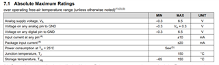
1.  What is the maximum source impedance?  Section 9.1.1 shows a 500 ohm ohm resistor and a 26pF capacitor and 4pF input capacitance.  If this combination is to be charged during Tacq = 350ns within 5 time constants, the total impedance is 2.3K, so the source impedance is a maximum of 1.8K.  Are my assumptions correct?

2.  Is the center pad connected to GND or floating?

3.  Can the voltage on Vin be higher than VA if the current is limited?  If yes, what is the maximum current?

  • Hello, 

    1. The ADC081S021 is a SAR ADC, which means the input is a switch capacitor circuit, this means the input impedance is dynamic and relies on the sampling rate the device is being used at. 

    2. The center pad should be grounded

    3. your understanding here is correct, though note that it is against the Abs max. It is not advised to have this as a reoccurring or consistent use case, this can decrease the life of the device. Instead this should be considered a protection method for a fault condition. Note the Abs Max states there is a 10mA max current limit to any one pin, we suggest closer to 2 mA for a current limit. 

    Regards

    Cynthia

  • The voltage won't change during Tacq = 350ns.  Are my assumptions correct? 

  • I do not understand your question

    If you are asking about question #3, if the input voltage change during the Tacq ?

    When Vin+0.3V>VA, the internal ESD diodes will turn and redirect the input current to VA, it is suggested that the power source to VA will be able to sink this current. If this case occurs during Tacq the device will measure a positive full reading.

    If you are asking regarding #1, if the input voltage will change during Tacq due to the dynamic impedance. During Tacq the input signal needs to charge the ADC internal sample and hold capacitor. How well the input circuit does this during Tacq will determine the accuracy of the ADC measurement.

    Note the image below, taken from a training video available online: SAR and Delta Sigma Basic Operation. The input signal must drive this signal within Acq time. When S1 open, the conversion phase begins and the input signal is no longer connected to the internal circuit of the ADC. this switch happens based on the sample rate/ clock rate the ADC is used at. 

  • The questions was about #1:  the voltage won't change during Tacq = 350ns.  Are my assumptions correct? Can I use a source impedance of 1.8K?

  • I suggest you review the  SAR and Delta Sigma Basic Operation ~click here~

    Can you share your schematic? what sample rate with the ADC operate at?

  • Slide 10:  assuming that Vcsh(t0) = 0V (i.e. S2 does its job), the equation reduces to:

    Vcsh(t) = Vin * (1 - e^(-t/(Rsh*Tsh))).  If t/(Rsh*Tsh) = 5 (five time constants, as mentioned above), Vcsh(t) = Vin * 0.993.  This is not quite 1/2 LSB, which is Vin * 0.998 for 8 bit resolution.  6 time constants is also not enough, but 7 time constants will provide Vin * 0.999.

    So (Source Impedance + Rsh) * (Csh + Cpin) * 7 < Tacq

    Source Impedance < Tacq / ((Csh + Cpin) * 7) - Rsh

    Source Impedance < 350E-9 / (30E-12*7) - 500

    Source Impedance < 1.1K

    Please double check my assumptions and math.

  • The snippet below is from Analog Engineer's Pocket Reference Guide. The table shows the time constants needed to settle based on the resolution, note that for 8 bit resolution, it will need 5.5 time constants. 

    Your math looks correct.