This thread has been locked.

If you have a related question, please click the "Ask a related question" button in the top right corner. The newly created question will be automatically linked to this question.

DAC5687-EP: Spurs on DAC output in carrier sweep NCO mode

Part Number: DAC5687-EP
Other Parts Discussed in Thread: DAC5688

Dear TI,

We are currently using DAC5687-EP on one of our Software Defined Radio Design and we encountered some trouble with the DAC5687-EP.

It seems that we have spurs with a frequency equals to fs/4 at the output of the DAC. We are using the DAC in NCO mode and set the sine frequency from 36.08MHz to 56.08MHz using a constant at the data input of the DAC.

The DAC input clocks are set to 192.86MHz in dual clock mode (CLK1 generated by an FPGA and CLK2 generated by clock source). We make a sweep of the DAC output frequency from 156.78MHz (192.86 - 36.08MHz) to  136.78MHz (192.86 - 56.08MHz).

The DAC registers are set to:

VERSION: 0x03
CONFIG_0: 0x02
CONFIG_1: 0x32
CONFIG_2: 0xc0
CONFIG_3: 0x80
SYNC_CNTL: 0xe0
SER_DATA_0: 0x00
SER_DATA_1: 0x00
NCO_FREQ_0: 0x55
NCO_FREQ_1: 0x55
NCO_FREQ_2: 0x35
NCO_FREQ_3: 0x3a
NCO_PHASE_0: 0x00
NCO_PHASE_1: 0x00
DACA_OFFSET_0: 0x00
DACB_OFFSET_0: 0x00
DACA_OFFSET_1: 0x00
DACB_OFFSET_1: 0x00
QMCA_GAIN_0: 0x00
QMCB_GAIN_0: 0x00
QMC_PHASE_0: 0x00
QMC_PHASE_GAIN_1: 0x00
DACA_GAIN_0: 0x00
DACB_GAIN_0: 0x00
DACA_DACB_GAIN_1: 0xff
DAC_TEST: 0x00

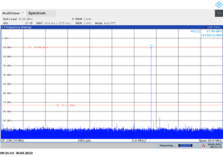
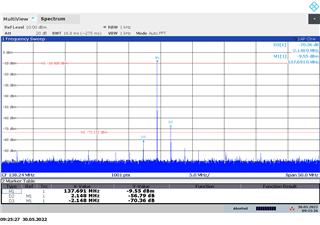
At 147.081MHz (span 50Mhz): The spur is not visible

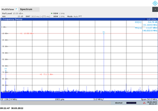
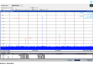
At 146.032MHz (span 50MHz): The spur is visible at 131.863Mhz

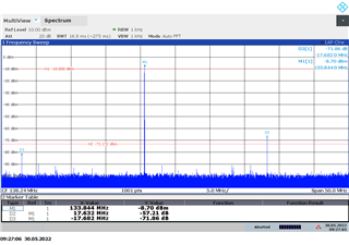
At 139.788MHz (span 50MHz): The spur and its mirror are seen (at : 133.544MHz and 146.082MHz)

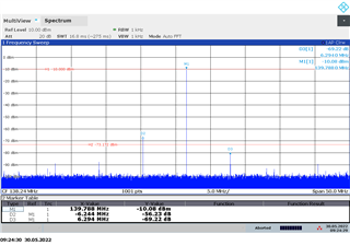
When we continue the sweep: we saw that the spur get closer to the output frequency of the DAC and then it go in the other direction when the frequency is crossed

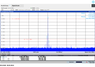
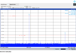
The spurs level are too high for our application ( >60dBc) and we cannot explain this behaviour of the DAC as it is out of the characteristics explain in the datasheet.

Can you explain this spurs or are we using the DAC in a bad configuration ?

Regards,

Kévin

  • Kevin, sorry for the delay. One of our experts will begin to look into this for you shortly.

  • Hey Kévin, 

    Based off your register map, (CONFIG_0 specifically), you are not using any interpolation or the PLL, meaning the DAC clock is running at the input rate. 

    Are you clocking both clock inputs with the same clock frequency? (192.86MHz). 
    It would appear if your sample rate is 192.86MSPS then the frequencies you are referring to are in the second Nyquist zone. (FS - NCO is the aliased image in the second Nyquist zone of the NCO tone). The output power you have is quite high for 2nd Nyquist however. Typically a sample and hold DAC is used in its first Nyquist zone (up to FS/2) as the output power is typically much lower in the second Nyquist zone. 

    I have a few questions. 

    1. Are both CLK1 and CLK2 receiving the same frequency (192.86MHz) from two different sources? (FPGA, CLK source). 
    2. Have you considered using interpolation to double the sample clock so you can operate in the first Nyquist zone? 

    Thanks!

    Matt 

  • Hello Matt,

    Thanks for your answer, to respond to your question:

    We confirm that we are using the DAC in direct mode (no interpolation). 

    1. Yes, both clock are running at 192.86MHz (coming from same oscillator and synchronous);

    2. Unfortunately, we can only run the sample clock up to 240Mhz which is too low our data [130.74;145.74]MHz;

    Do you mean that it is forbidden to use 2nd Nyquist zone with this DAC ?

  • Hey Kévin, 

    Typically with sample and hold DACs you want to operate in the first Nyquist zone as the images in the second Nyquist zone will be lower in output power and therefore your SNR, and other specs will suffer. Here is a great Application Report you can read that explains the output characteristics of a sample and hold DAC.

    https://www.ti.com/lit/an/slaa523a/slaa523a.pdf?ts=1654612171448&ref_url=https%253A%252F%252Fwww.google.com%252F

    The DAC you are using has a built in PLL/VCO that can double the sample rate to 385.72MHz internally You will still only need to provide the 192.86Mhz sample rate and the DAC will insert samples automatically using Sinc interpolation. I was able to get a similar setup to yours working on the DAC8588EVM I have in house. I will provide the configuration file to you to see if it helps. A few notes. 
    1. You should provide a single low phase noise clock to CLK1 and CLK1C. Based off your setup, a single clock is only needed. CLK2 and CLK2C can be left floating. 

    2. For the PLL to lock on the DAC5688 I used an N (ref) divider of 2 and M (FB) divider of 4 to set the PFD frequency to 96.43MHz. This makes the VCO then run at 385.72MHz, this is the final clock the DAC uses. 

    3. From there you need to configure the DAC to run in 2x interpolation mode. The DAC will insert samples between each sample provided using SinX/X (sinc) interpolation. From there your DAC will run at a full 385.72MHz. Try setting your NCO based off that new sample rate.

    Hope this helps!

    Matt

    One final thing, this configuration file is for a DAC5688 and not DAC5687-EP. There are some differences between these parts so you may need to tweak some more. 


    PLL_192p86to385p72.txt
    Texas Instruments Inc.
    DAC5688 EVM Register Configuration
    
    DAC5688 Registers
    Address	Data
    00		83
    01		C9
    02		01
    03		00
    04		98
    05		12
    06		00
    07		00
    08		24
    09		90
    0A		5E
    0B		42
    0C		00
    0D		00
    0E		00
    0F		24
    10		00
    11		00
    12		00
    13		00
    14		00
    15		04
    16		AA
    17		10
    18		80
    19		00
    1A		0D
    1B		FF
    1C		00
    1D		19
    1E		30
    
    CDCM7005 Registers
    Address	Data
    00		005FF1F0
    01		028282DD
    02		D00000A2
    03		00000027