This thread has been locked.
If you have a related question, please click the "Ask a related question" button in the top right corner. The newly created question will be automatically linked to this question.
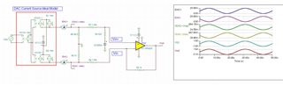
I'm looking at using a current source DAC (such as the DAC3164) feeding a voltage-feedback buffer amplifier (such as the OPA625).
The application calls for a unipolar output (0.1 to 1.6V out). It's desired to power the buffer amp from 3.3V.
Looking at SLYT360, it is straightforward to set up the amplifier for the proper input impedances, gain etc.
What is not covered (and what I need help with) is deriving the circuit changes needed to provide offset such that I can use the full resolution of the DAC over the output voltage range. I think this means that an offset needs to be fed to the buffer amp stage to bring the output to roughly 0.8V when the DAC output is at midrange.
Hi Nate,
Let me reach out to our amplifier team on this. I will update you as I receive info. Stay tuned.
Thanks, Chase
Hi Nate, please find our op-amp expert's comment below:
Sure this should be doable without too much complication. Assuming it's set up in a standard difference amplifier configuration, we'd just need to add an offset voltage to the non-feedback sides resistor that is usually grounded. I can send over a circuit if that doesn’t make sense. We’ll of course have to account for any DC output of the DAC as well.
Please let me know if having a circuit drawn out will be helpful for you.
Regards, Chase
That does make sense and I would appreciate a schematic. This is a high-speed node so how this gets tied back to the reference voltage generating the offset is important.
Nate,
I will ask for a schematic for you. Kindly await a response.
Thanks, Chase
Hi Nate,
Apologies for the delay, our amp expert was out of office. Please find his comments below:
I may have to rescind my earlier statement. The reason being is that this DAC has an output compliance range of -0.5 to 1V, which means that we would have to have the offset voltage below -0.5V in order to allow the DAC to meet the maximum compliance range. The only way I see this working is if we provided a separate negative voltage to terminate the DAC initially through a resistor and then our offset voltage to the amplifier. However, the math to do this starts to get quite ugly.
At this point I may just suggest it would be easier to use a first stage for converting the DAC output to a voltage and then a second stage to provide the offset.
Regards
Thanks for this advice.
I did a quick simulation, it seems marginally OK (DAC compliance voltage reaching 0.96V). I did no optimization on the design, so it is possible I could tweak the termination resistors and buffer gain to make that a little better.
The goal is to operate on a single 3.3V supply. If offset isn't provided in the first stage, then the first-stage buffer has to have a bipolar supply so it can swing below ground.
I think what I need to implement is called a "reference buffer". Do you have some circuit suggestions? It may need to source a few mA.
Nate, I've forwarded this to our amplifier expert for his suggestions. I'm also moving this thread to our amplifier team for faster support. Thanks
Hello Nate,
Chase has forwarded the thread over to us on the high speed amplifier group.
Would you happen to be able to share your simulation file or a snippet of the simulation circuit?
You most likely will need a dual supply configuration. Below are some resources on the setup for an amplifier interfacing with a current sourcing DAC.
Thank you,
Sima
I appreciate the link to the DAC buffer amplifier setup resources.
These don't include how to set up offset in the buffer stage to allow shifting the signal output over the DAC current output range to ~0.1 to ~1.6V (1.5V swing is required).
Referring to Figure 17 of SLYT368:
R1 and R4 = 249 ohms
R3 and Rf = 562 ohms
R1 and Rg = 499 ohms
I am proposing that offset of roughly 0.85V be injected by a positive voltage applied instead of ground at R3. Combined with the signal range, it should be possible to do this function with a RRIO op amp running from a single 3.3V supply.
(These values are chosen to demonstrate the option and are not compensated to make the DAC voltage swing equal.)
One could say this expands my requests:
Thanks for your help!
Hello Nate,
Thank you for the additional explanation!
The design is feasible and you will avoid violating the common-mode input of the amp, but you are correct it will alter the impedance calculations due to the varied reference. Here are some resources:
I will need to verify this in simulation, and will get back to you within the next few days.
Thank you,
Sima
Sima,
I would like to check in on this topic. You mentioned verifying this circuit in simulation and having a reply in a few days.
Best Regards,
--Nate
Hello Nate,
I apologize I missed the follow up to this thread.
Below is the a proposed design, but due to the lack of the negative reference, you won't be able to go down to -0.5V at the output of the DAC:
I mostly used these two references:
Thank you,
Sima
Thanks for this information! If I wanted to adjust the compensation to help with capacitive loading on the output (typically by adding a capacitor across R2), do I need to similarly add a capacitor across R4? Is there an appnote to suggest how this is done so that the 2 input impedances are balanced?
Best Regards,
--Nate
Hello Nate,
How much capacitive loading will be at the output? Usually we would recommend to compensate for this by adding an isolation resistor which will act as a RC filter. But, it depends on how much voltage drop (reduction in DC accuracy) is acceptable in your application.
Thank you,
Sima
20pF or so, not a lot. It's driving a mux and some input capacitance.
One other reason for the compensator is to help shape the gain peaking. Transient response is important in my application.
Best Regards,
--Nate
Hello Nate,
Specifically for OPA625, Figures 5, 6, 14, 15, 16 cover the effects of various load capacitors on the device. For better transient performance, you want minimal peaking in the frequency response which will correspond to less ringing or overshoot in the transient response. From the figures, 20pF is relatively small for this device. You can probably get by with 0 to 5 ohm isolation resistor. I will need to run a stability check just to be sure.
Thank you,
Sima