This thread has been locked.

If you have a related question, please click the "Ask a related question" button in the top right corner. The newly created question will be automatically linked to this question.

ADS8900B: Data acquisition using 6 ADS8900 : SPI communication

Part Number: ADS8900B

HI. 

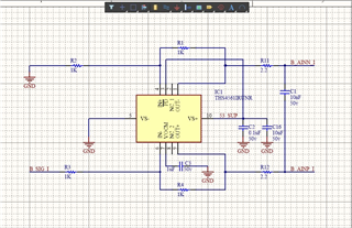
   I am trying to do SPI communication with my ADS8900 custom board, my strategy is as follows. 

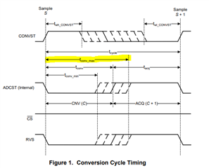
1. with rising edge of sampling clock. CONVST pin is pulled low.

2. Host controller/ FPGA  moniotrs the RVS pin for a rising edge.

3. With the rising edge on RVS pin host contrller pulls low the CS line and provide 22 serial clock to th ADS8900 sclk pin.

(basically fig 47 zone 1 data transfer)

1. My question is what should i actually send through the SDO pin (like can i send 0x67A89) to collect the 20 bit sample in SDI3 pin of the ADS8900 ? some data is given in data sheet (page no 27) but i am not clear with my understaning.

2. Can I power  6 ADS8900B with a single TPS7A4700 IC ?

regards

-----------

Pratik

  • Hello Pratik,

    1. My question is what should i actually send through the SDO pin (like can i send 0x67A89) to collect the 20 bit sample in SDI3 pin of the ADS8900 ?

    Keep SDI pin 22 low during the data conversion read frame, or 0x000000h

    I assume you are talking about the FPGA SDO output (MOSI), or the ADS8900 SDI pin 22.  In the case of reading the conversion result, keep the SDI pin 22 (MOSI) of the ADS8900B low during the frame.  The ADS8900 will interpret this as a No Operation (NOP), and simply return the most recent conversion result.  Unless you configure the ADS8900B for dual or quad SDO, then the output will always be on SDO-0 (pin 20).

    2. Can I power  6 ADS8900B with a single TPS7A4700 IC ?

    Yes, TPS7A4700 is rate for 1A (1000mA).  6x ADS8900B would need a maximum current of 36mA.

    Each ADS8900B will use a maximum of 6mA; 6x ADS8900B would use 36mA maximum.  The TPA7A4700 is rated up to 1A and can easily supply multiple ADS8900B, along with external input amplifiers and references.

    Regards,
    Keith Nicholas
    Precision ADC Applications

  • Hi...

       I  tried to put 0x0000 in the SDO line of the master.

    and provide (AnP - AnN = 2.5) to the differential input  and get the following data at SDO-0  : 0x2F7904

    I am not clear with the datasheet : how to decode this hex value to get 2.5v. 

    Regards

    ----------

    Pratik

  • Hello Pratik,

    The value that you are reading back is close to -2.5V.

    If you are providing a differential input of 2.5V, and using a reference voltage of 5V, then you set AnP=3.75V and AnN=1.25V, which will give a differential voltage of AnP-AnN=3.75-1.25-2.5V, and a common mode voltage of (AnP+AnN)/2=(3.75+1.25)/2=2.5V=Vref/2.

    The first 20b read from the data are the conversion result.  The last 2 bits are parity, and should not be used in the result.  The actual conversion result sent back (assuming I read your waveform correctly) is 0xBDE81h.  This suggests that you have applied a negative differential input to the ADC.

    0xBDE81h is in 2's compliment coding, and translates to -270719 decimal.  The calculated input voltage will then be:

    Vadc-in=Vref*Code/2^19=5V*-270719/524288=-2.582V.

    Regards,
    Keith

  • thank you Nucholas,

        My Logic Analyzer  didn't read data correctly, now i am able to understand.

    And Actually I was providing a input of +2.5 V but it was reading -2.5V,  and it is due to, I am supplying signal to IN- of the diff-opamp and IN+ to gnd (Shown in diagram). If i invert the connection I will get +2.5v right ?

    regards

    ---------

    Pratik

  • Hello Pratik,

    Yes, you are correct.  The diff-opamp inverts the input as you have shown.  Supply -2.5V to the B_SIG_I input in your schematic, and the ADS8900B should read +2.5V.

    Regards,
    Keith

  • Hi..

      I want to drive 6 ADCs .. and do simultaneous sampling . So my strategy is to club (SDI, CONVST, CLK, CS pins of all ADC together - like  CS_1 to CS_6 in one CS pin of master --- CLK_1 to CLK_6 in one CLK pin of master and so...)

    but 6 different SDO pins for ADCs (SDO_1 SDO_2 .... SDO_6) and 6 different RVS pins (RVS_0 RVS_1 .. RVS_6)

    After giving CONVST signal to ADCs ..Master will wait for 6 RVS pin to go high individually. and then issue CS low and following SCLK and SPI communication and collect ADC sample data from 6 different SDO pins. 

    will that strategy will be ok for simultaneous sampling ?

    regards

    ----------

    Pratik  

  • Hello Pratik,

    Yes, this approach will work.  An alternative to monitoring 6 different RVS pins is to wait the maximum conversion time of 670nsec for the ADS8900B, which will guarantee all RVS pins go high.

    Regards,
    Keith

  • Thank you. Keith