This thread has been locked.

If you have a related question, please click the "Ask a related question" button in the top right corner. The newly created question will be automatically linked to this question.

ADC3663: FCLK error in DDC bypass

Part Number: ADC3663

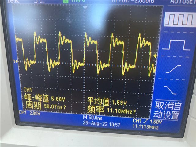
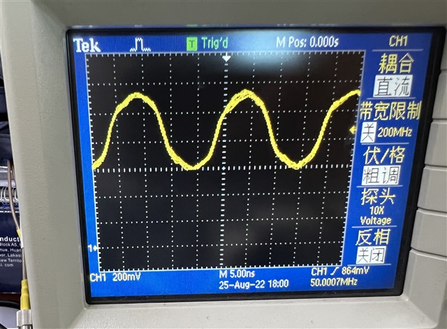
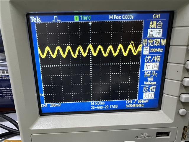
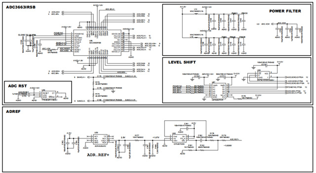
Hello, I am using ADC3663 and the settings are as follows when sampling at 50MHz: 2wire, 16bits, and DDC set to bypass, CLK input clock is 50MHz, and DCLK input clock is 200MHz.  However, the FCLK clock output by AD is not 25MHz and its duty cycle is not 50%.  Then other sampling rate tests are performed as long as DDC uses bypass, It is found that the FCLK output of AD is not a clock signal with a duty cycle of 50%, while the extraction rate of DDC is set to 2 or other normal.  May I ask what register setting error may cause this phenomenon?

  • Hello,

    One of our experts will be in contact within the next day. In the meantime, can you please provide images of what you are describing for the output of the ADC FCLK? This will allow our expert to assist better.

    Regards

  • My description is a little wrong. The duty cycle of FCLK is right, but the frequency is wrong. At 50M sampling rate, FCLK should be 25M, but the actual value is 11.1M.

  • Hello again, 

    Thanks for providing this image. I just wanted to request the input clock source details. Is this coming from some signal generator or clock synthesizer? I know this may sound strange but can you verify that the sample clock is indeed 50MHz and is not some 22MHz? Also note that the ringing shown in the image is likely due to the oscilloscope probe's ground lead and is not a concern.

    Regards

  • Hello,

    Thank you very much for your reply.I measured the input clock signal with oscilloscope, MCLK and DCLKIN are generated by SI5338.MCLK is a stable 50M, but DCLKIN has jitter and low amplitude although its frequency is 200M.At this time, the frequency of FCLK is 11.1M as shown in the image above, and all the data output by ADC3663 is 0.
    MCLK's image is below:

    DCLKIN's image and video are below:


    Regards

  • Hello,

    Thank you providing all of the captures. The duty cycle of the FCLK can be adjusted using registers 0x20 through 0x22 (Table 8-27. Register 0x20/21/22 in the ADC366x datasheet). Let us know if you continue to have issues and we can set up a test in the lab.

    Regards,

  • Hello,

    My original problem is that all the output data of ADC3663 is 0 in bypass mode (no decimation), but it is normal in non-bypass mode. I just changed the bit6-4 of 0x25 register. The picture I provided above is only intended to inform that the FCLK frequency is incorrect when MCLK is correct but set to bypass mode. So my problem is still not solved. I don't know which register setting error may cause this phenomenon. Please forgive me for not describing the problem clearly at the beginning.
    Regards

  • Hello,

    Using an ADC3663EVM in our lab, I setup and configured it (2w, 16b, bypass, 50M Fs / 200M DCLK) and measured a 25MHz FCLK signal and 50% with a scope. It is interesting that this is not an issue for you in decimation modes. Would it be possible for you to provide us with your schematics?

    Regards, Amy

  • Hello,

    The following is the schematic of ADC3663 and clock source respectively.

  • Hello,

    I have exported the required register writes for 2w, 16b, bypass and uploaded them here: 

    https://tidrive.ext.ti.com/u/nPz-LHN8_jiO_P4p/848f1700-d933-4dab-a932-9142e72a5004?l 

    Please compare your register writes to ensure that they are all correct.

    Regards, Amy

  • Hello,
    Thank you very much.  Now the data is normal at 50M sampling rate.  At 50M sampling rate 0x24 register must be set to 0, originally I set 0x6.
    However, I do not understand why bypass mode fails when DDC is enabled. And I tested that when writing register 0x24 to 0 (DDC disable), writing any value to bit6-4 of register 0x25 did not work.
    It feels like bypass mode doesn't do anything.

    Regards.

  • Hello,

    Bypass mode does not involve decimation or complex mixing, meaning that the DDC is bypassed. You are correct, bypass mode will only display the spectrum from DC to Fs/2. Glad to hear that your data is normal at 50M sampling rate now. 

    Regards, Amy

  • To add to what Amy said above, decimation is used mainly for reducing the data rate to your FPGA/MCU/DSP, which is helpful in a few ways. Firstly, this eases the requirements on the data processing side. Secondly, if the data of interest is within a small portion of the full nyquist zone, then only send that portion of the captured data - think of it as sending only the data you want, rather than sending all of the data, and then throwing away the data that you never needed to begin with. Bypass mode is when the decimation filters are bypassed meaning the register to enable the decimation filter has to be disabled. If the decimation filter is enabled, then you are operating in a real-decimation mode. If operating in a mode using the decimation filter as well as the NCO and down-conversion mixer, then this is a complex-decimation mode. These parts only operate in a single mode at a time. 

    Regards