This thread has been locked.

If you have a related question, please click the "Ask a related question" button in the top right corner. The newly created question will be automatically linked to this question.

ADC3663: ADC3663 Problem Support

Part Number: ADC3663

Hi team,

Use ADC3663 with 2-wire mode, 16bit output. There are some problems:

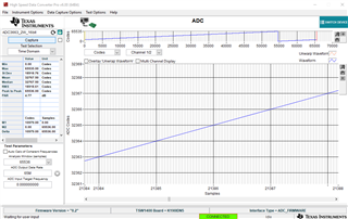
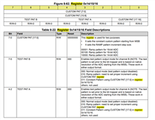
1.How to configure below three registers to output an increasing sequence, with a difference of 1 between each number?

2.What is the function of bit mapper?

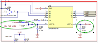
3.The SPI interface between the ADC3663 and the FPGA uses a level translation chip(TS0108E-Q1/TSB0108), but the high and low levels of the chip are not normal, and it feels like it is caused by the pull-down resistance inside the ADC3663 SPI pins. If you have any comments about this problem? Thanks.

  • Hi,

    The test pattern is set using Register 0x16. Writing data 0x48 enables test pattern mode, but the test pattern output does not become active until the increment size is set using CUSTOM_PAT[17:0]. For ADC3663 in 16-bit mode, this is set using pattern 00100 in CUSTOM_PAT[17:0]. Writing data 0x04 to register 0x14 will accomplish this. See the attached image to confirm this is what is desired.

    The bit mapper sets the output order of the data bits. There is a default configuration that gets loaded by default. It can also be manually changed using the unique identifiers and the appropriate registers.

    Regarding the comment on the SPI interface level translator, what do you mean the levels are not normal? Would you be able to help me better understand what the question or problem is here?

    Best regards,

    Drew

  • Hi Drew,

    Regarding the comment on the SPI interface level translator, what do you mean the levels are not normal? Would you be able to help me better understand what the question or problem is here?

    Now the FPGA is 2.5V level, the ADC3663 is 1.8V level, the ADC3663 SPI is 3-wire, and the data lines are bidirectional. so a level-shifting chip is used in the middle. However, the SPI pins of the ADC3663 have pull-up or pull-down resistors. Now, the SCLK SDIO of the four ADC3663 are in parallel, so it does not match the level translation chip. Is there a recommendation solution for suitable bi-directional level translation chip?

    If bit mapper is not enabled, can the ADC3663 output data normally? Thanks.

  • Hi,

    I assume you are referring to register 0x1B for the Mapper Enable bit? By default, the default configuration should already be loaded and the device will output data in that mode. The mapper enable bit is then only used to change the resolution of the output when in bypass mode. Does this answer your bit mapper question?

    On our EVM, see the below example for how we level translate from the FTDI to the DUT. The same concept can be used for an FPGA as opposed to FTDI.

    Best regards,

    Drew