This thread has been locked.

If you have a related question, please click the "Ask a related question" button in the top right corner. The newly created question will be automatically linked to this question.

ADS54J20: Clock connections from LMK0482x to FPGA (ADS54J20 + DAC37J82)

Part Number: ADS54J20
Other Parts Discussed in Thread: DAC37J82, , LMK04828

Hi!

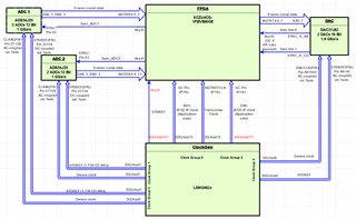
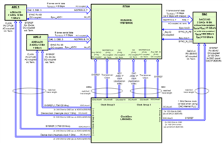
We have a new project where we want to connect two ADCs and a DAC via JESD204B with a Xilinx Ultrascale+ XCZU4CG.

I read several information about JESD204B already, but I have still some questions especially about connecting clocks from LMK0482x to FPGA.

Our plan so far:
- MPSoC XCZU4CG-1FBVB900E
- LMK0482x PLL / clock cleaner
- 2 x ADS54J20 devices (4 ADCs)
- ADC LMFS configuration 8224. So 8 lanes at 5 Gbps per ADS54J20 device (16 lanes in total).
- 1 x DAC37J82 (2 DACs)
- JESD204B subclass 1

My questions:
- Do we have to connect the "device clock" to MGTREFCLKxP/N or to FPGA clock pins (GC, QBC)?
- I read that SYSREF must be connected to FPGA clock pins. But to which clock pins? Do they have special requirements like GC or QBC clock pins at a HP bank or would HDGC clock pins on a HD bank be fine?
- Does SYNC need a general I/O on HP bank or would any pin on a HD bank be fine? Should it be located in the same bank as the SYSREF clock?

Best regards,

  • Hi Andre,

    I will have someone reach out to you shortly on this to provide guidance. Please give me a day or two.

    Thanks,

    Rob

  • Hi Andre,

    The FPGA needs two clocks from the LMK: one to the MGTREFCLK pins and one to a GC class pin (differential). The second one drives the application (sample) side of the JESD IP.  If the DAC and ADC line rates are not the same, you will need a third clock, to another GC pin. 

    SYSREF is not used as a clock, and can be connected to any pin. It needn’t be in the same bank as the GC clock pin. The same applies to SYNC. 

    One point about the SYNC pins is that if they are differential you may need to carry out external termination/biasing if you choose a bank that doesn’t support the required signal levels. 

    Regards,

    Ameet 

  • Andre,

    Also follow the routing guide info attached. The device clock and SYSREF trace lengths for the DAC should match but do not have to match the length of the ADC or FPGA clocks.

    Regards,

    JIm

    Subclass 1 clock routing.pptx

  • Hi Rob, Ameet and Jim,

    Thank you very much to all of you for help and information!

    The following is somewhat confusing: Most documentation shows a "device clock" and "SYSREF" from the ClockGen to the FPGA. But as I understood from Ameet, there are two clocks from the ClockGen to the FPGA (MGTREFCLK and JESD IP clock) plus the SYSREF which is not a clock at the FPGA side.

    I have inserted our current planning status here as a graphic. The SYSREF connection between the ClockGen and the FPGA is somebit unclear for me. On the ClockGen side it should be a SDCLKout, correct? And on the the FPGA side any single IO pin? This sounds wrong for me.

  • Andre,

    Ameet will help with the FPGA clock questions. Make sure to AC couple the data lines between the FPGA and ADC & DAC. This is not mentioned in your diagram.

    Regards,

    Jim

  • Hi Ameet,

    Thank you for your help! Can you please take a look at my answer below in this thread? Thank you!

    Regards,
    Andre

  • Hi Andre,

    Please confirm the line rates for the DAC JESD as well. You had mentioned that the ADC JESD lanes are 5Gbps.

    You will typically use DCLKOUT* as the clock sources for all the devices in the system (including the FPGA's MGT reference clock and the application reference clock). Please note that you may need two application clocks and two MGT reference clocks for the FPGA (based on your ADC and DAC line rates).

    For SYSREF, you will typically use SDCLKOUT*. These are all differential. Once again, you may need separate Tx and Rx SYSREFs to the FPGA (depending on the period of the multi-frame on each side).

    Regards,

    Ameet

  • Dear Ameet,

    thank you very much for your further help!

    The line rates for the DAC have not yet been finalized. There are two possible rates for us:

    • fDATA = fDAC = 1 GSa/s (no interpolation, fSERDES = 5 Gbps)
    • fDATA = 800 MSa/s, fDAC = 1.6 GSa/s (x2 interpolation, fSERDES = 4 Gbps)

    Therefor we will route the Device Clock (DCLKOUT) and SYSREF (SDCLKOUT) as well as the MGTREFCLK (DCLKOUT) two times from the LMK0482x to the FPGA as you wrote to remain flexible.

    I think we are almost done with the preliminary planning.

    • I wonder why at the ADS54J20EVM demo board the SYSREF signals are AC-coupled between the LMK04828 and the ADC. Shouldn't these be DC-coupled?
    • Do you see any disadvantages if we use SYNC_N_AB + SYNC_N_CD instead of the differntial SYNCB on the DAC37J82? The CMOS levels of the SYNC_N_AB/CD would allow us to use simple HD IO pins with CMOS levels at the FPGA.

    Please have a look at our updated diagram below.

    Best Regards

    Andre

  • Andre,

    SYSREF can be either AC or DC coupled. When using DC coupling, the user must make sure the common mode voltage is set properly and this can require extra parts depending on the device driving this input and the voltage standard used. The LMK does not specify a minimum for the LVDS option, and the typical value was near the lower end of the ADS54J20 LVDS specs. This is one reason we chose not to DC couple SYSREF.

    The only advantage I see regarding the single-ended vs differential SYNC is the single-ended requires one less trace.

    Regards,

    Jim 

  • Hi!

    Thank you very much for the further information and clarification!

    Best Regards,
    Andre