Other Parts Discussed in Thread: DAC8775
Hello, This is Naveen, I'm working with DAC8775EVM, Its a quad channel DAC.
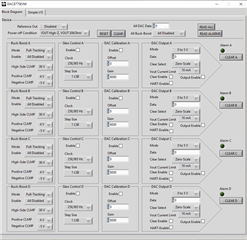
I configured
Ch1 as 4-20mA,
Ch2 as 0-10V,
Ch3 as 0-5V and
Ch4 as 0-20mA

Jumper and power connections are
JP1 to JP8 I’ve kept inside position.
JP9 and JP11 are installed and JP13 isn’t installed.
AVDD = +15V.
AVSS is connected to ground.
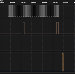
DVDD is powered through USB-DIG.Outputs at channel for Input FFFF are,
Ch1 – 7.471 (4 - 20 mA)
Ch2 – 7.33V (0 -10V)
Ch3 – 3.903V (0 - 5V)
Ch4 – 7.15 (0-20 mA)
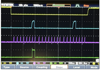
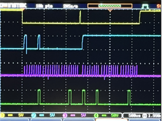
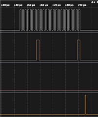
I was probing in at Vout on corresponding channels, I see inaccurate voltage and current in output.
I disabled one channel and tried to read the all other three channels by toggling in Output Enable, I see correct Voltage and current on Vout.
When I configure 4 channels right, the input supply drops to Vin/4. i.e. Vin = 15, so 15/4 is
its 3.8V but for three channels, the output fed to EVM remains as +15V.
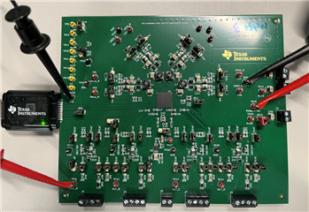
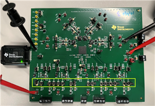
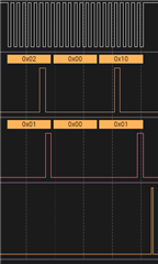
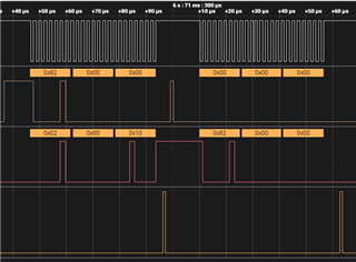
Please find the GUI and EVM connection settings.


Thanks,
Naveen