This thread has been locked.

If you have a related question, please click the "Ask a related question" button in the top right corner. The newly created question will be automatically linked to this question.

ADS7960: 8-bit transfers doesn't seem to work

Part Number: ADS7960
Other Parts Discussed in Thread: ADS8860

Hi,

I have used the above part and was successfully written/read using 16-bit transfer mode. However, when I tried to do the same with 8-bit transfer mode, it doesn't seem to work. The only difference between the two modes is that I have about 7.6uS gap between two 8-bit clock cycles. The CS remains low during the entire two 8-bit cycles. The MOSI data is valid as well. 

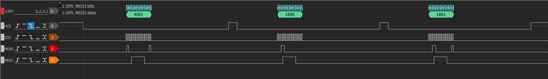
Following is the 16-bit cycles, which work. (All three cycles shown)

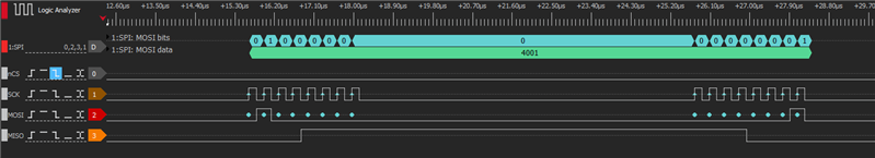
This is the first 8-bit cycle

As far as SPI is concerned, both should be valid. I couldn't find any timing parameter from the ADS7960 data sheet, which could explain this. As far as I can see, we are having a long setup time between 8th and 9th clock cycles. 

Any ideas?

Cheers,

Kaushalya

  • Kaushalya,

    I reviewed the timing section and I also do not see any parameter that explicitly says that the clock needs to be symmetrical.  However, many similar devices do have this specification.  For example, ADS8860 shows that clock low and high time need to be roughly symmetrical (see below).  

    The ADS7960 data sheet shows all communications in 16 clock groups with symmetrical clocks, so there is an implication that this is what you should do.  It seems that your design is working well with the 16 symmetrical clocks.   Is there a reason why you need the gap?

    Best regards,

    Art

  • Hi Art,

    Thanks for your reply. I think the 8 bit mode is also working similar to 16 bit version. The only thing was after sending 0x4001, 0x1800 and 0x1801 in the initialization, I have to send 0x1801 again to turn on the GPIO!! Do you see any error in the initialization data send?

    The SCLK 50% duty cycle is not a requirement of ADS7960 as far as I can see from the data sheet. So I think the 8 bit mode should be fine.

    Cheers,

    Kaushalya

  • Kaushalya,

    My understanding is the following:

    1. You are configuring DIO3=INPUT, DIO2=INPUT, DIO1=INPUT, and DIO0=output.  You do this first.  (0x4001)
    2. You then select channel 8 in manual mode and set DIO0=0.  (0x1800)
    3. You then select channel 8 in manual mode and set DIO0=1. (0x1801)
    4. For step 2 and 3.  The status of the output will update in the frame after the current frame.  For example in step 2, you set the DIO0=0.  You will see this take effect in the next frame.  For GPIO that are configured as inputs, the input status is latched on the falling edge of the CS in the current frame and displayed on SDO in the current frame.
    5. Maybe the delay you are seeing is the delay I mention in item 4 above.  In otherwords, you don't see the output untill the next frame.  This behavior is documented at the bottom if figure 50.

    I hope this helps.  Let me know if you have further questions.

    Best regards,

    Art