This thread has been locked.

If you have a related question, please click the "Ask a related question" button in the top right corner. The newly created question will be automatically linked to this question.

ADS8363: Full-clock mode related question of ADS8683

Part Number: ADS8363

Hi team,

My customer has a question regarding the full-clock mode of ADS8683.

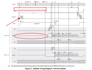
When the IC /CS signal is enabled, there is a rising edge of CONVST, but SDI and RD seem to be ignored and take no action according to the pin function, and SDO is a tri-state, so they want to know what is the exact function of SDI, RD and SDO this in this mode? (Looking at the timing diagram, the difference between the full clock mode and the half clock mode is mainly concentrated here). So they want to know the mainly difference between full-clock mode and half-clock mode.

Regards,

Xiaoying

  • Hi Xiaoying,

    The main difference between full-clock and half-clock mode of the ADS8363 is when you read the conversion results.  As depicted in Figure 2 above, CONVST is applied and the conversion results are output after BUSY goes low when the conversion is complete.  /CS and RD need to be applied in order to start the SDOx shift.  Contrast that to Figure 1 - in half-clock mode, the previous (note data n-1 label on SDOx) is output while conversion 'N' is on-going.