This thread has been locked.

If you have a related question, please click the "Ask a related question" button in the top right corner. The newly created question will be automatically linked to this question.

ADS4229: Timing constraint in FPGA for data aquisation from ADS4229

Part Number: ADS4229

Dear engineers from TI,

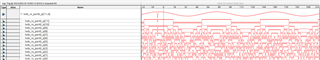
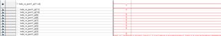
our group bought ADS4229 from ti to build up a board for signal covertion from analog to digital, we use Altera FPGA board to receive the data from the ADC, the chip is configured as CMOS mode, and adc clock is at 250Mhz and send from FPGA. As under CMOS mode the clock cannot be sent back to FPGA, so the data received in FPGA some times may face timing violations. My question is how can i know the violation is exatly what type, and how can i solve it by adding timing constraint.

Thanks & Best regadrs,

Minshanserveral bits get abvious wrong data according to timing violation

  • Hi Minshan,

    I'm not sure I follow why the CLKOUT cannot be used as the data clock for receiving ADC data. Is this just to share a common clock domain inside the FPGA? Without using the CLKOUT to latch the data, there is no way to know whether the data is latching early or late. This device has delay adjustment on the CLKOUT but nothing for delay adjustment on the input CLK.

    Thanks, Chase

  • The best option is to connect the CLKOUT to the FPGA if your design has this option designed in. If not, does your FPGA allow for any kind of phase offset adjustment when creating the PLL?