A related question is a question created from another question. When the related question is created, it will be automatically linked to the original question.
If you have a related question, please click the "Ask a related question" button in the top right corner. The newly created question will be automatically linked to this question.
LMP92066: GaN negative voltage monitoring using LMP92066
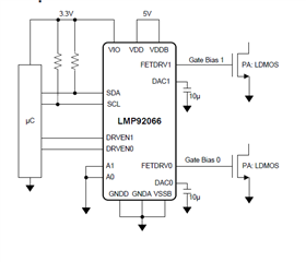
I am using LMP92066 for GaN negative gate bias voltage control. What are the changes I need to do for the circuit shown below to control the negative bias control for GaN PA.
The only change you would need to make to the circuit is to apply GND to VDDB and apply -5V to VSSB. This will set the DAC and FETDRV outputs to negative voltages. All of the other circuitry should be the same.
Yes, the LMP92066 is limited to only one output range, since the maximum differential voltage between the VDDB and VSSB is 5.5V. You would need to use two different devices in order to bias both a GaN PA and an LDMOS PA.
One more question for clarification is that, if I use LMP92066 for GaN negative bias circuit, then both VDD and VDDB has to grounded right ? You mentioned only to ground VDDB before so wanted to confirm whether both VDD+VDDB should be connected to ground.
VDD controls the analog circuitry in the chip, while VDDB controls the voltage of the DAC buffer. In this case, you would want to keep applying the positive 5V to VDD to keep the part working as intended, while grounding VDDB to ensure the DAC buffers operate in the negative range.
We decided to use LMP92066 bias controller circuit in our design. As we are using GaN PA and it needs neg gate bias voltage to come first before dc power is applied to drain of PA so that PA is not damaged. Do I need any other circuit after bias controller circuit so that GaN PA is not damaged? When we power up bias controller TI iC, does the bias voltage output from the chip is close to -5V (equal to VSSB and how long does it stay at -5V so that PA is off during initial power up.
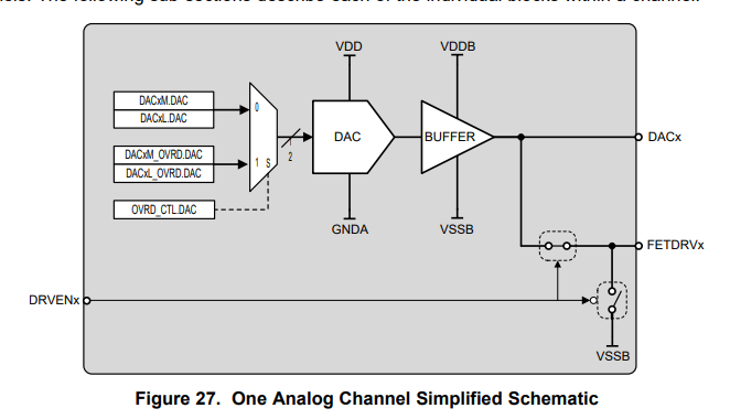
At startup, the DACs are pulled to the VSSB line, -5V. So the PA will be turned off. When the ALU and LUT start up, they will force the DAC to the programmed code. By default, this is code 0, so the DAC should stay around -5V until it is written to a new voltage.
1) The reason I am asking because GaN PA supply voltage will be connected as soon as we power up the device. So the DACS have to be -5V before the supply to PA is connected in order not to blow up the PA. If there is a delay in applying -5V DAC to PA before the supply voltage is connected then this can damage the PA. Any thoughts on it.
2) But AMC7904 has some internal control to sequence this but do not think LMP92066 has that. I am using 4 LMP92066 in our design and wondering whether any of your customer has controlled GaN power sequencing using LMP92066.
3) Can we stay at code 0 for longer time if we want so that DAC stay at -5V longer.
1) This is a valid concern. First, I'd like to confirm the setup for the IC Output. You should be connecting the GaN Gate to the FETDRVx pin. The DACx output should have only a capacitor connected to it. As you can see in the block diagram, the FETDRVx pin has two switches. One connects to VSSB and the other connects to DACx. At startup, the switch connecting FETDRVx to VSSB is closed, meaning that the pin will output -5V. The DACx output will startup in whatever way the ALU was programmed (with a factory reset part, this will be code 0, or -5V.) When the control pin DRVENx is driven high by your host controller, the FETDRVx switches to the DACx output. Applying a low voltage to the DRVENx pin switches the FETDRVx back to VSSB.
So, at startup, the FETDRVx pin will stay clamped to VSSB -5V until you switch it to the DACx voltage using the DRVENx pin.
So, going back to your questions:
1) The FETDRVx pin will ramp to -5V as VSSB ramps to -5V. If you apply the IC power at the same time as applying the GaN PA Drain power, you will have a small amount of time where the GaN PA is on due to the ramping. In this situation, we would recommend applying the GaN PA Drain power later than the IC's power or create a control circuit using some external circuitry that keeps the GaN PA Drain voltage from being applied until you enable it.
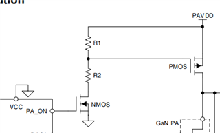
2) Correct, the AFE10004 has a PA_ON pin to control the PA Drain voltage, but it still requires some external MOSFETs to control.
Here's an example of that circuit from the Application Report on the AFE10004 page. In this circuit, the Drain voltage (PAVDD) needs the PA_ON pin to be high in order to be applied to the GaN PA. You could do something similar in your setup, but with a signal from your host controller. The LMP92066 does not have any pins that can do this on its own.
3) The FETDRVx pin will be clamped to -5V until you apply a high voltage to DRVENx, after which the FETDRVx pin will be clamped to the DACx voltage.