This thread has been locked.

If you have a related question, please click the "Ask a related question" button in the top right corner. The newly created question will be automatically linked to this question.

ADS131M08: DRDY not going low

Part Number: ADS131M08

Hi,

I am working on ADS131M08 using Verilog. The steps followed are as below:

After power-on:

1. START/SYNC driven to low wait for 2050 ADC CLK cycles (adc_clk = 8.8181 MHz generated from FPGA IP) with CS high

2. Reset de-asserted and waiting DRDY rising edge

3. Set CS low and wait for 2 ADC CLK cycles

4. Disable all the channels

5. Set MODE register = 16'h0100

6. Set GAIN1 register = 16'h7777

7. Set GAIN2 register = 16'h7777

8. Set CLOCK register = 16'hFF8A

9. Disable CS (high) and wait for 2 ADC CLK cycles

10. Wait for DRDY falling edge and enable CS (low) & wait for 2 ADC CLK cycles

11. Send read command to read CLOCK register only

12. Send 9 dummy words and disable CS and wait for 2 ADC CLK cycles

13. Wait for DRDY falling edge and enable CS & wait for 2 ADC CLK cycles

14. Read CLOCK register

15. Send 8 dummy words and disable CS and wait for 2 ADC CLK cycles

16. Repeat steps 10 onwards

The SCLK = 20 MHz (generated from FPGA IP). Following the above steps I am finding the DRDY signal = 1 all the time.

Would you let me know the reason for this?

Thanks & Regards

Prakash

  • Hi Prakash,

    Are you supplying an external master clock to CLKIN?

    Best regards,

    Dale

  • Hi Dale,

    Yes. Through FPGA and generated from IP.

    Regards

    Prakash

  • Hi Prakash,

    Thank you for your confirmation.

    You should be able to see the /DRDY pulses after the ADC is properly powered up without writing registers. Also, to read a register, there is no need to check the status of /DRDY output signal.

    To address your issue, could you provide the following information?

    • Your schematic.
    • For test purpose, do not write any register and just read a register(e.g. MODE register) after your ADC is powered up, provide a timing captured with a logic analyzer for SCLK, /CS, DIN and DOUT signals. Two-frame timing is needed to check because your register will be shifted out in next frame.

    Regards,

    Dale

  • Hi Dale,

    I had requested for friendship to share my schematic. Please do accept it.

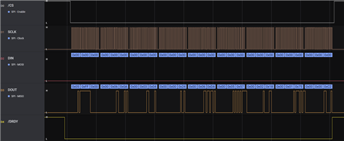
    Mean time I am sharing you the results for reading clock register after powering-up the ADC. Would you review and let me know?

    Below image indicates the 2 frames data (between first blue marker to yellow marker). Second blue marker is the start of second frame.

    The below image is for sending write command to read clock register.

    This image shows the event occurring on DOUT line in between dummy clocks before completion of the frame.

    The above images are captured with SCLK = Fclk/2. And it is being observed same with SCLK = 20 MHz. The response is not as expected I feel. Please do let me know the reason for it.

    Regards

    Prakash

  • Hi Prakash,

    I will look into it and get back to you soon.

    Regards,

    Dale

  • Hi Dale,

    I had mailed you the schematic.

    Sure.

    Regards

    Prakash

  • Hi Prakash,

    Did you keep /CS always low? 

    Below the right timing to read CLOCK register, note that you can just send RREG command with 24 SCLKs in the 1st frame and you can see the register data (0xFF0E) in 2nd frame by sending another 24 SCLKs, there is no need to send 9*24 SCLKs in a frame for reading a register:

    The 2nd timing below is writing CFG register with WREG command: 

    The 3rd timing below is reading data for all channels, the data on DOUT:  Status register+CH1 data+CH2 data...+CH8 data:

    I hope these timings can help you understand. 

    Your schematic looks good, but you do not have common-mode capacitors on inputs and also I do not know your purpose to use two 1kohm resistors between AINxP and AINxN.

    Regards,

    Dale

  • Hi Dale,

    Thanks for the response.

    Good news...... I am glad that my code is working. The changes I made are:

    1. After RST de-assertion I started writing to the registers directly instead of disabling the channels.

    2. In earlier code I was writing the registers one after another with full command (e.g. {WREG_CMD, CLOCK_REG_ADDR, 7'd0, CLOCK_REG, 8'd0} = 48 bits) having some delay in between and with /CS low. It didn't work. Now, I modified as send write command for writing 4 registers (24 bits) and after few clocks of gap register value (24 bits) one after another with few clocks of gap in between and kept /CS low.

    But why it didn't work earlier I am unable to make out. If you any idea let me know.

    Does /CS require to toggle between writing a register with complete command (48 bits)?

    Schematic:

    What is this common-mode capacitors? Where do they require to be added?

    I asked about 1kohm resistance between inputs to my designer, he said that he had referred to a reference circuit and from there it is derived. Surely, I am unaware of it.

    Regards

    Prakash

  • Hi Prakash,

    For your item 2, I did not fully understand what your full command is, is the following format your full command?

    • "WREG command (011b) ->CLOCK register address(000011b)->"0000000b" + "CLOCK_REG data?(16 bits?)" + "00000000b".

    If so, where is your delay? also, this format has total 40 bits, not 48 bits. Please clarify.

    Can you please explain "toggle between writing a register with complete command (48 bits)"? 

    If you exactly follow my timings above, you should not have any trouble to write, read registers and also retrieve conversion data.

    For the schematic, the common-mode capacitor is the capacitor between input and AGND, usually its value is the differential capacitor value*(1/10).

    Regards,

    Dale

  • Hi Dale,

    Full command means {WREG_CMD, CLOCK_REG_ADDR, 7'd0, CLOCK_REG, 16'd0} = (011b)+(000011b)+(16 bits data)+(16 bits '0').

    Sorry, it is not 8 bits but 16 bits. So in total it will be 48 bits.

    There is no delay between the words. I didn't find any information about the delay between 2 words in the datasheet. Would you let me know how much min and max required timings between write words?

    Toggle between the words: I meant that /CS low till complete write of 1 register and high for few cycles. Then again drive low for next register write and high, so on till all the registers are written.

    For schematic: Do I need to connect this coupling capacitor between (AINxP and AGND) and (AINxN and AGND) or (AINxP and AINxN)?

    Input to the ADC is a differential. So, please clarify.

    Regards

    Prakash

  • Hi Prakash,

    Your full command for writing a register to M08 ADC is incorrect. Since your word size is 24-bit, so you have to send your both WREG command and data in 24-bit format. Your total WREG command+data should be: 

    • 1st 24-bit word:   (WREG_CMD) + (CLOCK_REG_ADDR) + (7*'0' for single register write) + (8*'0') = (011b)+(000011b)+(0000000b)+(00000000b)     
    • 2nd 24-bit word:  (CLOCK_REG) + (8*'0'} = (16-bit register data) + (00000000b)      

    You can have a delay between these two words, like one SCLK delay in my WREG timing example I showed to you above, or there is no problem to send out all 48-bit data to the ADC if there is no delays between the words. I strongly recommended you to see my timing examples above.

    Toggle between the words: you can write your registers one by one by toggling the /CS signal for each frame, or you can write multiple registers in a same frame by keeping the /CS low until all register data are sent out, see the timing in the figure 8-25 in the page 45 of the M08 datasheet. Note that the 'nnn nnnn' in your WREG command should match the quantity of the register in your frame of both solutions.

    For schematic:  both differential and common-mode capacitors are helpful to filter noise. I would recommend you to check the details in the FAQ for selecting RC component value and the cutoff frequency of anti-aliasing filter:

    https://e2e.ti.com/support/data-converters-group/data-converters/f/data-converters-forum/955466/faq-delta-sigma-adc-anti-aliasing-filter-component-selection

    Regards,

    Dale

  • Hi Dale,

    Thanks for the response.

    I do agree with you on the command. I also will try following the timings as mentioned by you considering at least one SCLK delay between words.

    I also try by keeping /CS low till I write all the words and check.

    Regarding the schematic I had shared the information to my design engineer, and he will look into it.

    Now, when I am using the SCLK with 20 MHz, I am getting the resolution of ADC as 10 bits rather 13 (13.4 as per datasheet) for the above configurations I mentioned earlier. But at the same time if I reduce SCLK to 10 MHz I am getting the resolution as mentioned in the datasheet. What would be the reason? How does SCLK decide the resolution of ADC?

    Regards

    Prakash

  • Hi Prakash,

    Are you working on the same project and case as the following thread for a bridge application?

    ADS131M08: ADS131M08

    If so, see my response in that thread. Note that you should correct your commands first by following my suggestions.

    Regards,

    Dale

  • Hi Dale,

    Yes, both of us are working on the same project. He is looking into hardware and I am into FPGA coding.

    Sure, I will look into.

    Regards

    Prakash

  • Hi Prakash,

    Please keep posting the queries from both of you on the same thread because it's the same project/device, thanks.

    Best regards,

    Dale

  • Hi Dale,

    Sure.

    Regards

    Prakash