This thread has been locked.

If you have a related question, please click the "Ask a related question" button in the top right corner. The newly created question will be automatically linked to this question.

ADS54J69: output is not detected from LMK04828

Part Number: ADS54J69
Other Parts Discussed in Thread: LMK04828, ,

Dear TI experts,

My customer now tests ADS54J69 with LMK04828 and xilinx FPGA (use JESD204B)

the block diagram is as below;

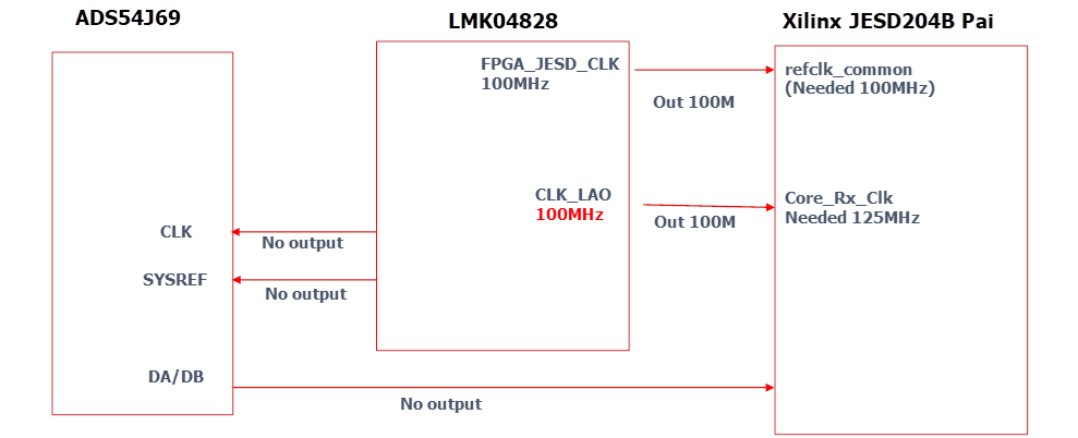
They confirmed FPGA_JESD_CLK as 100MHz. (it is okay)

and changed Clkout 12 and 13 DCLK Divider from 30 to 24 -> confirmed 125MHz output. (is it right to fix this configuration?)

the problem is they could not see the output from DCLKOUT2 and SDCLKOUT3 of LMK04828.

attached file is the configuration of GUI. Could you check the settings and find right configurations for these outputs?

ADS54JEVM.pdf

Please let me know if you need more information about it. Thanks.

Best regards,

Chase

  • Chase,

    Is this with the ADS54J69EVM or a custom board? If it is a custom board, what is the frequency of the OSC input to the LMK? Is the PLL2 locked on the LMK?

    Regards,

    Jim

  • Dear Jim,

    Thank you for your support.

    - It is customer's own PCB, but almost they made same as EVM.

    - OSC input is 100MHz. EVM has 125MHz but they changed it to 100MHz

    - Yes, locked LED is on, so PLL2 is locked.

    and my customer tested more. here are the results.

    1. they applied these 2 cfg files.

    6886.ADS54J69_2x_dec_lowpass_4222.cfg

    8787.LMK_Config_Onboard_1000_MSPS_FPGA_100M.cfg

    2. they changed CLK12 out divider : 30 to 24.

    3. they set register 69000 test mode(bit4) activated for test mode.

    4. after they measured 4 sample/125MHz of xilinx JESD204B output. the result is on the page 4 of ppt file below. please check this output is right or not.

    JESD_Test_PAT.pdf

    Please check this issue. Thanks.

    Best regards,

    Chase

  • Chase,

    The JESD_TEST pattern should be 0x0001, 0x0002, 0x8000, 0x8000, 0x8000, 0x8000, 0x8000, 0x8000, that repeats. The config files look correct. 

    Make sure to issue a hard reset to the ADC after power and clock is present but before writing to the ADC registers.

    Regards,

    Jim

  • Dear   Jim,

    Thank you for your support.

    my customer tested jitter pattern.

    What is your tested pattern? it is not like my customer's results. Could you guide me to get your results?

    Best regards,

    Chase

  • Chase,

    This is the pattern I see out of the ADS54J69 when writing a "1" to bit 4 of page 0x6900 address 0x00. 

    I am now retired from TI and will forward this post to another engineer in our group in case you have any other questions.

    Regards,

    Jim

  • Dear manager,

    Because Jim has retired from TI, so I hope someone will support this thread.

    1. my customer tested JESD_TEST pattern as Jim said, but they got different result.

    -> 0001 0000 8000 8000 8000 8001 8000 8000 8000 8001 ... (repeated) data is different also cycle is different.

    2. They set ADC sample rate as 500MHz(2ns) and 125MHz(8ns X 4 samples) on Xilinx Pai chipset. the result of gt0/gt1 is as below;

    I think it is also different from the pattern we expected.

    3. Is there any way to test to verify the ICs are working properly?

    Best regards,

    Chase

  • Hi Chase,

    We will update you on Monday next week on what we find.

    Regards,

    Rob

  • Dear Rob,

    Thank you for your support.

    Please let me know if there are update about the issue above.

    and here are additional question from my customer ;

    1. Last time Jim said that the JESD_TEST pattern should be 0x0001, 0x0002, 0x8000, 0x8000, 0x8000, 0x8000, 0x8000, 0x8000 and repeats. Is it right?

    2. We found about DA0/1 channels in ADS54J69 datasheet. Could you tell me the sequence of JESD_TEST pattern in order of DA0/1 channels?

    Best regards,

    Chase

  • Hi Chase,

    Please reiterate the open issues on the new forum post for this.

    I will close this thread now.

    Regards, Amy