This thread has been locked.

If you have a related question, please click the "Ask a related question" button in the top right corner. The newly created question will be automatically linked to this question.

ADC128S102QML-SP: Junction to Board Thermal Resistance ADC128S102WGRQV (5962R0722701VZA)

Part Number: ADC128S102QML-SP

The language in the (E2E thread) thread below appears vague, and as it stands I would not feel comfortable stating that I now know enough about the 5962R0722701VZA part to start a thermal analysis that incorporates a thermal path between the part and PCB where it is installed.

There are a lot of assumptions that both the user and the TI tech are making, that may or may not be true of the 5962R0722701VZA part.

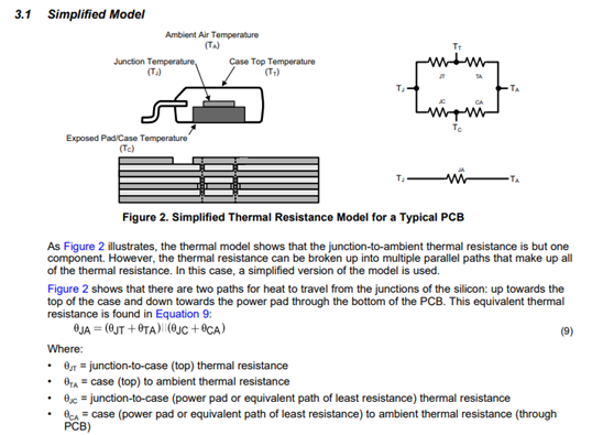
To assume the Junction-Board thermal resistance is the same as the Junction-Case thermal resistance, is impossible without test data or very detailed knowledge of the part's construction (i.e., perhaps the part's construction is highly symmetrical and the part leads do not participate as a significant thermal path??? I honestly have no idea, but perhaps TI does...).

Which leads to my question for TI, and I apologize for all the references that make this question look messy, but I mean to be very specific:

Is the Junction-Board thermal resistance the same as the Junction-Case (Top) thermal resistance (11.2 C/W per datasheet SNAS411P –AUGUST 2008–REVISED APRIL 2017, Sheet 6, Section 6.4) for the 5962R0722701VZA part (TI PN: ADC128S102WGRQV, 16-lead ceramic SOIC)?

Thanks,

Tim

  • Hi Tim,

    Short Answer:

    In general, I agree with you it doesn't quite tell the whole story. I wouldn't assume  R_θJC(top) = R_θJC(bottom). Let me see if I can put in a thermal modeling request for you.

    Long answer:

    To expand on Joselito's and Cynthia's response, R_θJC(top) and R_θJC(bottom) are parallel paths for power to dissipate. Depending on the layout of the board underneath, R_θJC(top) (called R_θJT in diagram below) and θJC(bottom) (sometimes called R_θJB) might be the dominant path where one overtakes the other (much like parallel resistors). The problem is that heat still needs to travel from the case to the ambient air which leads us to R_θCA(top) (or R_θTA in diagram below) and R_θCA(bottom). This is where something like a heat sink and thermal paste will reduce the R_θCA(top) and help with heat disipation.

    Unfortunately, I don't have much experience with ceramic packages but what I could find is that most devices I could find tend to have R_θJC(bottom) is less than R_θJC(top). But they are certainly different numbers.

    The bigger problem, is that the datasheet really only gives part of the story. You don't know R_θCA(top) and R_θCA(bottom) can really only be found out using expensive simulation technology. The R_θJA in the datasheet is R_θCA(bottom) + R_θJC(bottom) where R_θCA(bottom) is defined by a standardized layout defined in the JEDEC standard EIA/JESD51-x series of documents. Note, that we've taken a look at some of JEDECs layouts and they are a mix of good and bad. With good layout (like the thermal pad idea), its possible to get better than the R_θJA in the datasheet.

    Sometimes, R_θJC(bottom) is specified in the datasheet. For the ADC128S102-SP, it is not, and can't be back-calculated because R_θCA(bottom) is changed for every different type of device package. More info that you you probably wanted but hopefully helpful. Even more info on our testing can be found here: http://www.ti.com/lit/pdf/spra953 

    The way I prefer to do it is just build the board, test in the worst thermal case, and the use the ΨJB or ΨJT number after measuring it directly with a thermal camera. I realize how this might be a problem for these very expensive devices or ones that are buried within a system.

    I will also mention that this device is old, I'm not sure what kind obstacles we'll run into but I'll put in a request with the thermal modeling team. Depending on the workload, this may take up to month to get the numbers.

    Best,

    -Cole

  • Cole,

    Thanks for the reply.

    If it helps bring in the lead time, all I need is the R_θJC(bottom). This should be a simple conduction analysis.

    I do not need the R_θCA(bottom). Agreed the transfer to the air beneath the part would be more difficult to assess, and as such would likely only be useful in a narrow band of use cases.

    Tim

  • Hi Tim,

    Thanks for the information. I was able to submit the request, we'll see if there's any issues. I think the lead time has to do with the team's bandwidth (they got 15 new requests just today and they have a backlog). I'll keep you updated but at least we're in the queue.

    Best,

    -Cole

  • Hi Tim,

    Good news, looks like we already had the data, just not shared publicly on E2E yet (all C/W):

    Result- Theta JA-High K (standard datasheet value) 128.1
    Result-Theta JC, top (standard datasheet value) 70.4
    Result-Theta JB (standard datasheet value) 117.9
    Result- Psi JT (standard datasheet value) 49.4
    Result- Psi JB (standard datasheet value) 108.5
    Result-Theta JC, bottom (standard datasheet value) 11.9

    You might notice that the R_θJC(top) is now a new number and R_θJC(bottom) is the similar to what R_θJC(top) used to be. Essentially, the bottom number was put into the top slot by accident. Also, we have more accurate simulation model now so the value changed slightly. We've got confirmation to change it in the future but these are the correct values. I'm thinking about marking this as a FAQ just in case.

    Let me know if you have any other questions.

    Best,

    -Cole