This thread has been locked.

If you have a related question, please click the "Ask a related question" button in the top right corner. The newly created question will be automatically linked to this question.

ADS54J69: Please check the test pattern of ADS54J69

Part Number: ADS54J69
Other Parts Discussed in Thread: LMK04828

Dear TI experts,

My customer asked about ADS54J69 before, but response delays several days.

Could you check the status of this issue? The schedule is very urgent.

https://e2e.ti.com/support/data-converters-group/data-converters/f/data-converters-forum/1240436/ads54j69-output-is-not-detected-from-lmk04828

additionally, please check the other customer's project which is combined with FPGA. it would be very helpful if you give me some example about it.

Best regards,

Chase

  • Hi Chase,

    Yes I am checking into this. Jim retired so I am working to understand where he left off with the customer.

    Regards, Amy

  • Hi Chase,

    I am going to close the old post with Jim's feedback.

    For clarity moving forward, please reiterate open issues on this post.

    Thank you, Amy

  • Dear Amy,

    Thank you for your support.

    Actually we got 2 cfg files when my customer first started evaluation. Here are 2 cfg files below ;

    2604.ADS54J69_2x_dec_lowpass_4222.cfg

    8233.LMK_Config_Onboard_1000_MSPS_FPGA_100M.cfg

    first of all, my customer use ADS54J69, and JESD204B settings as below ;

    and Here are the questions ;

    1. Please check 2 cfg files that the whole settings are for ADS54J69+LMK04828 and JESD204B(IP of Xilinx FPGA) LMFS 4222 configuration.

    (my customer changed external OSC to 100MHz refer to other TI engineer's advice.)

    2. In the settings above, what is the expected frequency of CLK and SYSREF to ADS54J69 and FMC connector?

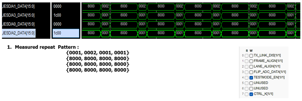
    3. "ADS54Jxx EVM GUI v1.8" SW was used to set test pattern mode bit (6900 bit4). The following waveform measured Xilinx JESD204B 4 lane data. Based on Figure 74 of ADS54J69 Datasheet, it was measured with pattern repetition as shown below.

    {0001,0002,0001,0001} {8000,8000,8000,8000} {8000,8000,8000,8000} {8000,8000,8000,8000}

    Is this measured data accurate? if not, What should be measured?

    Please check this issue. Thanks

    Best regards,

    Chase

  • Hi Chase,

    I have the setup in the lab, I will get back to you tomorrow with what I find.

    Thanks, Amy

  • Hi Chase,

    For question 1, Jim previously suggested switching to the 100M oscillator for their design to get this frequency, due to the dividers in the LMK04828. Additionally, I tested the ADS54J69 configuration file and was able to get a capture. Just for reference, I have attached the two configuration files here that I used to get a baseline capture.

    For question 2, the output frequencies will be based on the GUI settings / register writes required to configure the LMK04828 (under LMK04828 -> PLL2 Configuration in the GUI). For example - the frequency for the LMK04828_CLK to the FMC Connector - in our schematic is the oscillator is 122.88 MHz. Following the GUI block diagram, this frequency is multiplied by 12, and again by 2, and then divided down by 12, resulting in the 246.76 MHz frequency, which I then double checked on the scope. 

    For question 3, the test pattern I saw differed from the test pattern Jim saw, so I am going to check with our design team on this and get back to you.

    Regards, Amy


    7331.LMK_Config_Onboard_983p04_MSPS.cfg8688.ADS54J69_2x_dec_lowpass.cfg

  • Dear Amy,

    Thank you for your support.

    My customer summarized again about the issues. Please check the questions below.

    1. About ADS54J69 timimg

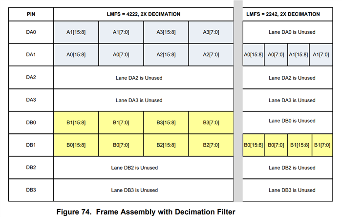
    What if LMFS4222 mode setting, only DA0/DA1 channel is used.

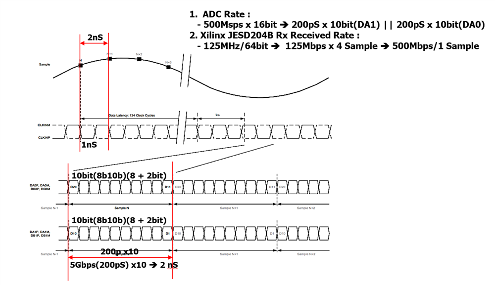
    Is it correct that each channel is 5Gbps/10bit serial output?

    2. About I/O configuration

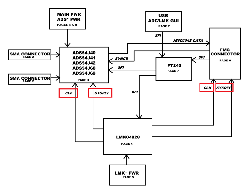
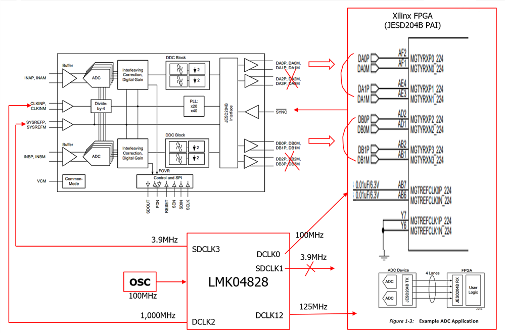
    ADS54J69 and LMK04828, Xilinx FPGA connection configuration is as below. Is it correct?

    3. About measuring clocks by 1Gsps oscilloscope

      - DCLKOUT0(FPGA_JESD_CLK) : Measured 100MHz

      - SDCLKOUT1(FPGA_JESD_SYSREF) : Measured 3.9MHz

      - DCLKOUT12(CLK_LAO) : Measured 100MHz, But I need 125MHz for Xilinx JESD204B Rx data stream. So, Changed “CLKout 12 and 13” by 32 -> 24

      - DCLKOUT2(CLK) : not measured/ May be 1GHz

      - SDCLKOUT3(SYSREF) : Measured 3.9MHz

      --> Please confirm that these frequencies are correct or not.

    4. About measured test pattern by Xilinx Logic Scope

    Please confirm that this test pattern is correct or not.

    Best regards,

    Chase

  • Hello Chase,

    Question 1:

    To understand this, please refer to Table 8 on page 36 of the datasheet.

    Running at the max 500 MSPS rate, the max fserdes rate will be:

    500 MSPS -> decimation by 2 -> 250 MSPS * 16 bit * 1.25 (8b10b) = 5 Gbps

    (Note that this is for both channel A and channel B, see datasheet Figure 74)

    Question 2:

    These frequencies look fine, just double check that they meet the requirements of the ADC and FPGA.

    Question 3: 

    I am still awaiting an answer from the design team on the expected test pattern, but I passed along your measured pattern.

    Thanks for sending that along. 

    Regards, Amy

  • Hello Amy,

    I am ASTEL dkkim who requested technical support.

    Are you sure that the four signals of Channel A (DA0/DA1) and Channel B (DB0/DB1) are transmitted to the FPGA at 5Gbps speed?

    FPGA uses Ultrascale+ Class, and JESD204B Pai IP is designed and operated in 5Gbps 4 Lane mode.

    After setting to ADS54J69 Test Mode, the already sent Xilinx Logic Probe Tool results are shown at a speed of 250Mbps.

    Could there be a setting related to this phenomenon in the ADS54J69, LMK04828 Chip setting Script File?

    I hope for a quick reply.

    Best regards,

    Dkkim.

  • Hi Dkkim,

    Table 8 on page 36 of the datasheet shows the max SERDES rate at 5 Gbps.

    Let me double check with the team on what could be causing you to see a speed of 250Mbps.

    Regards, Amy

  • Hi amy,
    Additional Test Pattern tests were  last week, and the results are as bellows.

    1. Page 0x6900, address 00, bit4=1, bi3 =1, result is 0x0001 repeted.
    2. Page 0x6900, address 02, data=0x20, result is 0xb5b5 repeted

    Are the above results correct?

    When will I receive a reply to the results of my previous request?

    Best regards,
    dkkim.

  • Hi Dkkim,

    I confirmed with the team that the SERDES rate should be 5 Gbps. Can you clarify what you are measuring? 

    Is it possible the tool you are using is actually measuring 250 MSPS, not 250 Mbsps? 

    If inputting the clock at 1 GHz then with decimation by 2 it would be expect that you would see 250 MSPS.

    I have tested this in the lab with the TI EVM, using a ~1 GHz sample clock with no issues. 

    I am still trying to get an answer from the design team on the expected test pattern, I should have an answer early next week.

    Regards, Amy

  • Hi amy,

    I am still waiting for the Expect test pattern data value.

    Question 1: Why does it take more than a month to check the Expect test pattern data value, which is one of the ADS54J69 features?

    Is there any additional documentation for ADS54J69 ? 

    This project is developed based on Xilinx's typical JESD204B Application and Ti ADS54J69 EVM Board.

    In the meantime, the development history is summarized as follows.

    1. We received LMK04828, ADS54J69 Register Script File from Ti to apply LMFS4222 Mode of ADS54J69.

    Question 2: The LMK04828 DCLKOUT12 is 100MHz.

                     In general, in 5Gbps/4Lane method, 125MHz x 4 Sample is required to receive 500MSPS Data.

                     Why did you deliver the script at 100MHz?

    Question 3: Please check the LMFS222 mode Script File that you sent to set the register again.

    1. For LMFS4222 Mode, we changed LMK04828 OSC(Y1) from 122.88MHz to 100.00MHz.

     This summarizes the development so far.


    To check the performance of Xilinx Serdes, I verified it as below through Xilinx ibert IP..

    As shown in the test result below, there is no problem with 5Gbps reception performance for each of the 4 lanes in Xilinx FPGA Serdes.

    Question 4 : Can you send me the verified results of the ADS54J69 Evaluation environment with the same environment (OSC.= 100MHz, DCLKOUT=125MHz) as the script you sent me ?

     I would appreciate your quick results.

     Best regards,

    Dkkim.

  • Hi Dkkim,

    I am still waiting on our design team to get back to me with an answer on the expected test pattern. 

    I previously set this up in the lab and provided you with the configuration file I used to get a baseline capture. However, our EVM uses a 122.88 MHz oscillator, so you will need to take that into consideration if you are using a 100 MHz oscillator due to the dividers in the LMK04828. If you are confused or need help programming the LMK04828, consider posting in the clocking forum for support. 

    However, I may be able to figure out a solution and will check into this for you.  

    Regards, Amy

  • Hi Amy,

    I have some questions about ADS54J69 input/Output.
    Question 1 : What is the voltage range supplied to the analog input(J3,J2) in the ADS54J69 EVM Evaluation environment?

    How does this signal relate to the VCM voltage?

    Question 2: Is ads54J69 16bit Digital output format Signed or Unsigned output?

    Can you please send me any technical documentation you have on these two questions?

    Best Regards,

    dkkim.

  • Hi Dkkim,

    Regarding your question on the test pattern:

    Please refer to the another similar post here for reference. Jim did a great job explaining the expected test pattern: https://e2e.ti.com/support/data-converters-group/data-converters/f/data-converters-forum/679520/ads54j42-ads-54j42 

    The K parameter is set to 16, meaning the the pattern will repeat every 32 samples in the 4222 mode. 

    I started here in the example at sample 32, and the pattern will repeat every multi-frame.

    On channel 1, the expected test pattern will read: 

    Samples 32-33 -> 0x0001 (representing Channel A)

    Sample 34 -> 0x0001 (representing sample 1 from converter 1)

    Sample 35 -> 0x0002 (representing sample 2 from converter 1)

    Samples 36-63 -> 0x0000, then repeats every 32 samples

    On channel 2, the expected test pattern will read: 

    Samples 32-33 -> 0x0002 (representing Channel B)

    Sample 34 -> 0x0001 (representing sample 1 from converter 2)

    Sample 35 -> 0x0002 (representing sample 2 from converter 2

    Samples 36-63 -> 0x0000, then repeats every 32 samples

    Regards, Amy

  • Hi Dkkim,

    To answer your other two questions:

    Question 1:

    -> The max differential input voltage is 1.9 Vpp (datasheet pg. 7) 

    -> The input signal will swing around the common mode voltage, VCM. 

    Question 2: Is ads54J69 16bit Digital output format Signed or Unsigned output?

    Table 39. Register 4Bh -> bit 5 (datasheet pg. 53) states "Default, output is in twos complement format"

    This can be changed to offset binary output if desired.

    Regards, Amy

  • Hi Amy,

    Thank you for your quick reply.

    I have analyzed the measured data for the Expected Test pattern you sent and the results are as follows.

    1. It is repeated every 32 samples.
    2. If you inverse the D15 bit of the measured data.   It is the same as the Expected Data you sent.

    1. There is a misalignment phenomenon when measuring data.

                The data as shown in the figure above is acquired with a probability of 10%.

                There is also a phenomenon that the bytes of each sample are swapped.

                Is there a method for stable alignment?

    1. Even in Non Test Pattern Mode(Analog Input), D15 Inversion and

               D15 Inversion and Unstable Align phenomenon is the same ?


    Best regards,

    Dkkim.

  • Hi Amy,

    I'll send you a remeasured plot file 

    The CH1 Expected Data sequence you sent is 0001, 0001,0001,0002,8000,8000... .

    In the Plot Data I sent you, the sequence is 0002,0001,0001,0001,8000,8000, ....

    The sequence is different.

    CH2 Expected Data sequence is 0002,0002,0001,0002,8000, 8000 ... Correct.

    What do you think about the above phenomenon?  

    Best regards,

    Dkkim.

  • Hi Dkkim,

    Yes I looked at your test pattern result and CHB looks good. However, it appears that CHA is inverted. The test pattern is correct, just inverted (read the opposite way, it is 0001 -> 0001 - > 0001 -> 0002. Please check the board routing of CHA. 

    The D15 bit is related to offset binary / two's complement format, depending on what format you use this bit will be a 1 or 0. 

    Regards, Amy

  • Hi Amy,

    Thanks to your technical support, the Expected Test Pattern and misalign issue have been resolved.

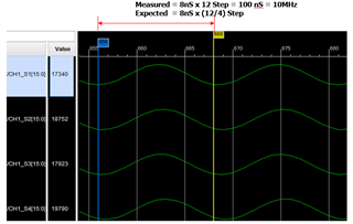
    In the case of inputting Analog 10MHz/1.0Vpp Sign as follows signwave.

    The waveform has an 8nS sample step. 

    All 4 samples S1, S2, S3, S4 are measured at 100nS(8nS x 12 Step).

    I thing that it should be measured in 1/4.

    What are your thoughts on the above happens ?

    Best regards,

    dkkim.

  • Hi Amy,

    Never mind my previous e-mails about expected analog signwave. 

    As shown below, when inputting 10MHz, 1.0Vpp Signwave,

    It was measured as a wave as shown below.

    Signwave is mesured at 100nS(10MHz) accurately with 2nSx50 Steps.

    As you known, CH1 Pattern abnomaly, the above issues were 4 sample order with Xilin 204B pai IP.

    All issues so far have been resolved.

    So, thank yoy again for your technical support.

    I wish you good luck.

    Best regards,

    dkkim.

  • Long time no see, Amy.

    The ads54j69 chip is operated under the same conditions as “Figure 73 Lane Alignment Sequence” in the “ads54j69 Datasheet”.

    As a result of the operation, there is a problem with synchronization of the data received from the FPGA.

    Is there any special method for stable operation?

    Best regards,

    DKKIM.

  • Hi Dkkim,

    Just circling back to the beginning of this post - your previous results showed that you were able to successfully capture the test pattern and input?

    Can you clarify when you say that there is a synchronization issue with the data received from the FPGA?

    Regards, Amy

  • Hi Amy,

    The Test Pattern obtained from the previous experiment is normal as shown below.

    ADS54J69 Analog input is mulfunction as shown below when inputting 1MHz, 1Vpp signwave.

    If the case of Test Pattern input is perfect, is it seen as a different problem rather than a synchronization problem?

    The Signwave output that I experimented with in the past is not being reproduced.

    In this case, what kind of problem do you think?

    Best Regards,

    DKKIM.

  • Hi Amy,

    This is additional information about the problem.

    The received Signwave shows the same characteristics, and certain parts of the data are also repeated.

    Is there a problem with the ADS54J69 Register setting?

    Best Regards,

    DKKIM.

  • Hi Amy,

    As a result of retesting in Test Pattern mode, 32 Sample should be repeated in LMFS4222 mode,

    but It is measured by repeating 16 samples.

    Note please.

    Best Regards,

    DKKIM.

  • Hi Amy,

    The previous problem is that the LVDS output amplitude of the LMK04828 DCLK12 is very small, less than 200mV.

    The above signal acted as an unstable phenomenon in JESD 204B PAI Main Clock of FPGA.

    There is no problem with the current operation, but I am worried about mass production in the future.

    LMK04828 Is there any setting or method to improve the LVDS output of DCLK12?

    Best regards,

    DKKIM.

  • Hello DKKIM,

    We are going to close this post, so could you please create a new one with this clocking question? Also, please make sure to attach your latest TICS Pro file or config file of the LMK04828 and your schematic to that post. Thanks in advance.

    Best,

    Andrea

  • Hi Andrea,

    How can I create a new Ticket?

    Can you make it and let me know?

    Best regards,

    DKKIM.

  • Hello DKKIM,

    Unfortunately, I can't create it because it needs to be made from your account.

    To create a new post, just follow the same process you used to create this one (they will be two completely different posts but that's what we want). On the new ticket, make sure to explain your question again and include your config (.cfg)/TICS Pro file (.tcs) and your schematic.

    Thanks,

    Andrea