This thread has been locked.

If you have a related question, please click the "Ask a related question" button in the top right corner. The newly created question will be automatically linked to this question.

ADS1115: INL test results mismatch with datasheet

Part Number: ADS1115

Hello,

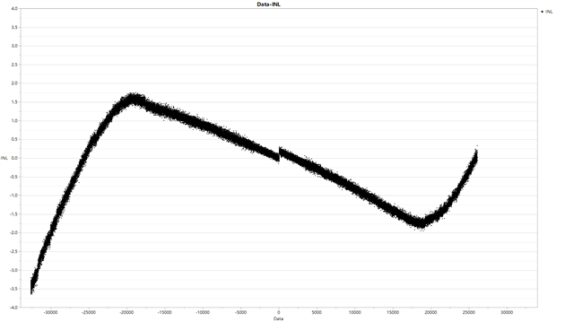
We did  the DAQ module with the ADS1115 and used it to do the INL test , but the results were not satisfactory and differed significantly from the values on the datasheet. We don't know where the problem is, and we hope the engineers can help us. The following are the experimental conditions:

Measurement Environment: Normal temperature, the ADC input RC circuit is the same as the EVM, the SMU gives the ADC a differential input signal and the DMM measures the input signal. Perform a ramp scan.

Chip settings: Select differential input, FSR set to ±2.048V, SPS=8.

INL calculation: Find the intermediate voltage that occurs with the same code, get a code-voltage curve, fit the curve using best-fit, and calculate the deviation of the curve from the line that fits to get an INL.

The picture shows our measurements, which do not match the values and graphs on the datasheet.

Best regards

Kailyn

  • Hi Kailyn,

    The INL test for the data sheet was not performed with the EVM, so using the EVM circuit for this test setup might cause slightly different results. 

    Can you provide us with more details on the setup used for this test? Was the part used in single-shot or in continuous mode?

    Can you provide more details on the SMU and the signal used for the measurement?

    I will consult this with the team. 

    Best Regards,

    Angel 

  • Hi Angel,

    This is my test result and Kailyn helped me post it here. Please let me answer your questions.

    We set chip in continuous mode and give a differential input.

    The SMU type is Keisight B2912A, setting resolution of SMU could be 1uV in ±2.048V. But we add 10uV every step in order to save test time.

    The DMM type is Keythley DMM7510, measurement resolution of DMM could be 1uV in this range. And the accuracy and linearity are enough to measure analog input of ADC.

    We don't have any ideas about what's wrong in our test, please help us check this result.

    Best regards,

    Jenks

  • Hello,

    The parts are thoroughly tested to meet data sheet specifications, so it is likely that the error is in the way the measurement is being taken. 

    What we suspect could be going on is that the offset and gain error are not being accounted for in the INL test that is being performed. 

    Two-point calibration should be performed to eliminate the gain and offset errors from the measurement. 

    On our TI precision labs series we have a video that goes into detail on the concept and math behind doing the calibration for these types of measurements. Please refer to the video titled "Understanding and calibrating the offset and gain for ADC systems" under the error sources section. 

    Analog-to-digital converters (ADCs) | TI.com

    We also noticed that to sweep from -2.048V to +2.048V at 10uV increments using 8SPS the test will take hours to complete.

    At an FSR of ±2.048 V the size of an LSB is 62.5 μV, which is bigger than the 10uV step increments. It is not possible for the ADC to detect such small changes in voltage in this FSR configuration. Less sample points at a bigger step size can be taken to for the test which would save test time without losing valuable information. 

    Just to clarify, what is being plotted exactly in the graph provided, output code (x-axis) vs deviation in LSB from expected output code?

    Is there a reason this test is being performed?

    The test after calibrating should give better results. I will see if I can find more information on the INL test.

    Best Regards,

    Angel 

  • Hi Angel,

    Sorry for the late and thanks for your answer.

    We think ads1115 was calibrated before delivery, so we don't think it is necessary to calibrate again. Is it necessary?

    The graph shows every output code(x-axis) vs INL(y-axis, calculated by best-fit method).

    Cause we want to design a DAQ module, so the INL of ADC is the most important characteristic that we care about. We want get the curve about code VS INL.

    Jenks

  • Hello Jenks

    The INL test takes into account the gain error and offset error of the device and accounts for those. It is likely that the total unadjusted error which includes the INL error, gain error and offset error is what is being measured by this test, and it is being attributed only to INL making it appear larger than our specification. That is why a two-point calibration to account for offset and gain error is necessary for accurately measuring the error produced only by INL.

    INL errors are unavoidable but gain error and offset error can be removed with digital calibration to reduce your total error.

    Two-point calibration can be done by taking a measurement at 10%FSR and 90%FSR then using these two data points you can generate a line of best fit and calculate the offset error in LSB at the 0-code crossing (think of the b term on a y = mx + b linear fit). This offset can then be added to the adjusted code. The same two-point data can be used to apply a gain correction coefficient to account for gain error. Gain error can be thought of as the difference in the linear slope compared to the ideal slope of the transfer function. 

    This technical article further explains these error sources. 

    ADC Accuracy Part 2: Total unadjusted error explained - Precision Hub - Archives - TI E2E support forums

    At the moment that is what I suspect could be the issue with the measurement.  

    Is the input ramp to the ADC being measured for accuracy?

    A schematic/diagram of the setup or the raw data could be useful to help determine if something else is causing problems in the measurement. 

    Best Regards,

    Angel