
This technical article was updated on July 23, 2020.
In the first ADC Accuracy post, we established the differences between the resolution and accuracy for an analog-to-digital converter (ADC). Now we can dig into the factors that contribute toward total accuracy of the ADC, often referred to as Total Unadjusted Error (TUE).
Ever wondered what “Total” stands for in the TUE specification of ADC? Is it as simple as adding up all the DCerror specifications from an ADC datasheet (i.e. offset voltage, gain error, INL) or is there more to it? As a matter of fact, TUE is a ratio of the total system errors with respect to the operating input range of the ADC.
More specifically, TUE is a DC error specification expressed in units of least significant bits (LSBs), which represents the maximum deviation between the actual and the ideal transfer functions of an ADC. This specification assumes that no system level calibration is performed (i.e. it's an unadjusted result). Conceptually, TUE is the combined effect of the following types of non-idealities in the behavior of an ADC:
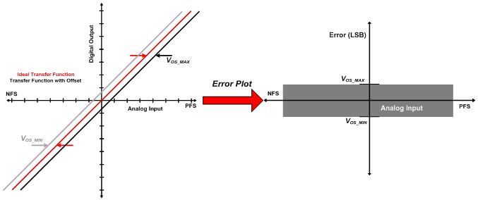
- Offset Error (VOS): The constant difference between the actual and ideal transfer curve of the ADC, as shown in Figure 1. It is the measured digital output obtained by shorting the ADC inputs to GND.
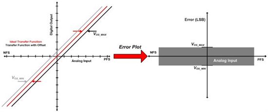

Figure 1. ADC Offset Error vs. Input Voltage
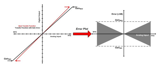
- Gain Error: The difference between the actual and ideal slope of the ADC output. It is usually expressed as a ratio of ADC range or maximum error at the full scale codes. As illustrated in Figure 2, the absolute value of gain error increases as the analog input approaches the full scale values.

Figure 2. ADC Gain Error vs. Input Voltage
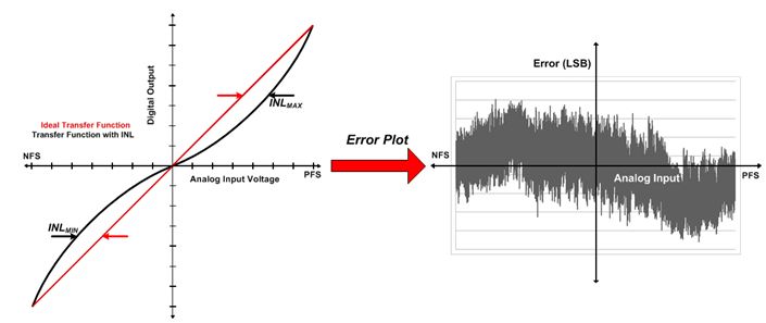
- Integral Non-Linearity (INL): The maximum non-linear deviation of the actual ADC transfer curve from the ideal straight-line behavior. The INL response of the ADC has no definite shape and depends on the internal circuit architecture, as well as distortion, caused by the front-end signal conditioning circuit.
Figure 3. ADC INL Error vs. Input Voltage
Most ADC datasheets specify the typical and maximum values for all the above DC errors, but not TUE. Calculating the maximum value of TUE is not as simple as taking the sum of the maximum values of all the individual DC errors. This is because all of these errors are uncorrelated, and in the worst case offset, gain and linearity errors may not all occur at the same input voltage on the ADC transfer function. Hence, a simple summation of errors may make the system accuracy look unnecessarily worse. This is especially true if the dynamic range of the application is limited near the middle of the transfer function.
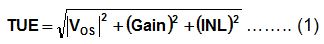
In a typical data acquisition system, there is an input driver and a voltage reference along with the ADC, both of which also contribute to the overall offset and gain error. Hence in most systems without calibration, offset and gain errors dominate INL for calculating the maximum value of TUE. A recommended way of calculating the maximum TUE at a particular analog input voltage is to take the root-sum-square (RSS) of the maximum values of all individual errors at that point ,(Equation 1). It is important to convert all of the errors into the same unit, usually LSBs.
Equation 1 yields a typical “bow-tie”-shaped error plot for TUE. For systems with higher offset error, the “bow-tie” plot has a thicker knot (Figure 4A). On the contrary, for systems with higher gain error, the knot of the “bow-tie” becomes thinner and the bows become thicker (Figure 4B).
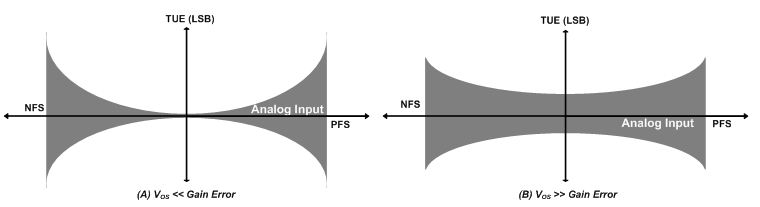
Figure 4. “Bow-Tie” Shaped ADC TUE vs. Input Voltage
In summary, there is no definitive formula to calculate the maximum value of TUE for an ADC because the error is dependent on the input range at which the ADC is being operated. If the system does not require utilizing the entire input range of the ADC, you can minimize TUE by operating the ADC away from the end points of its transfer function.
Related resources: