This thread has been locked.

If you have a related question, please click the "Ask a related question" button in the top right corner. The newly created question will be automatically linked to this question.

ADC34RF52: Input Clock Specifications

Part Number: ADC34RF52

Hello,

Would you clarify TI's definition of VID (differential input voltage) for the ADC34RF52 Clock input.  The spec indicated

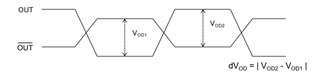
Is VID measured from signal itself as VOD seen below:

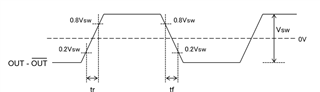
or is it measured as what is seen by the ADC's difference amp which effectively doubles the output swing when the input signals are summed:

I'm trying to determine the ratio of the step up transformer I should use to increase LVDS to approach the max spec of 2.4 Vpp

Thank you,

Joe

  • Hi Joe,

    VID will be measured as the difference between the positive and negative pair. The first image you posted shows this.

    For this device, the clock should be AC-coupled and is self biased at the ADC side, Each half of the differential clock input should swing a max of 1.2V around your shifted LVDS common mode. For instance, if you have an 0.8V common mode on each of the differential lines, each individual line should swing ±0.6V (0.2V through 1.4V). This creates a 1.2Vpp swing on the half of the differential signal. As each half of the differential pair is 180° out of phase, then the total differential voltage will be twice this, at 2.4Vpp. Does this help to clear up any confusion?

    Regards, Chase

  • Thanks, Chase.  So it comes down to each half of the differential clock signal must be equal or less than CLKVDD (1.2V) when measured peak to peak.  Is that right?

  • Hi Joe,

    Yes, this is correct, if you go by the max input level of the clock.

    I would suggest the clock level being lower than 1.2V SE on each clock leg and more in line with typical 1Vpp DIFF voltage instead as per the datasheet.

    Thanks,

    Rob

  • Hi Rob, the primary reason I'm interested in maximizing clock amplitude is from the TI article "Clock Jitter Analyzed in the Time Domain, Part 3".  Clock amplitude was shown to have a noticeable impact on SNR.

    In my case, I will be particularly sensitive to clock performance because I will be sampling 900 MHz at ~500MSps.

    Is there a potential problem if I push each half of the clock to the 1.2V SE max instead of the 0.5VSE (1Vpp Diff) voltage?

    Thanks,

    Joe

  • Hi Joe,

    As long as you are below the abs max ratings on the clock input pins, it should be fine.

    Maximizing slew rate of the clock will help, but only if the clock is clean to begin with.

    I would try a few experiments and "dial in" the right clock amplitude level based on your performance expectations.

    Regards,

    Rob

  • Sounds good.  Thank you, Rob.  Yes, it's very clean (25fs).