This thread has been locked.

If you have a related question, please click the "Ask a related question" button in the top right corner. The newly created question will be automatically linked to this question.

ADC128S102QML-SP: Control Register clocking

Part Number: ADC128S102QML-SP

Hello TI,

We are currently struggling with one of these component producing unexpected Data on one of our Electronic board.

Some timing issues might to be at work, but we would like some precision or confirmation we don’t find in the datasheet.


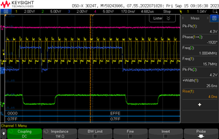
The following figure represents in red the way we are driving DIN ADC input:


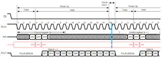
 Our understanding of the datasheet was that DIN pin hold and setup timings are to be respected only for the first 8 rising edges of each 16-sclk cycle.

 "While a conversion is in progress, the address of the next input for conversion is clocked into a control register
through the DIN pin on the first 8 rising edges of SCLK after the fall of CS. See Table 1, Table 2, and Table 3."

As you can see above the DIN pin (in RED) is stable for these 8 SCLK rising edge so no timing issue shall be observable there.
However we currently use the 16th SCLK rising edge (highlighted in blue) to update the DIN value for the next cycle.


Because this update happens at the same time of SCLK rising edge, we wonder whether there is a risk of setup/hold timings not being respected for control register clocking even if that happens out of the window of the first 8 rising edges.

Can this somehow lead to unexpected data output ?


Our first interpretation of the datasheet was that there was no control register clocking outside the first 8 SCLK rising edges of each 16-sclk access.

Can you confirm that point ?


Best regards,

  • Hi Jokin,

    Welcome to our e2e forum!  The MUX actually changes after the eighth rising edge so that it is ready for sampling (Track mode) on the falling edge of the next conversion cycle.  What sort of issues are you having?  Can you provide an screen capture of your /CS, SCLK, SDI and SDO?

  • I can:


    Red: N_CS
    Yellow: SCLK
    Blue: DIN
    Green: DOUT

    For this design, we are using ADC's continuous mode, that explains why N_CS is always low.
    The chan that is supposed to be selected on this screenshot for the next acuisition is chan N°5, and then chan N°0.

    For the first acquisition slot, DIN is effectively stable for the acquisition of the 8 control register bits "11101111" on SLCK rising edges where "101" corresponds to the actual usefull bits.
    For the 2nd acquisition slot, DIN is effectively stable for the acquisition of the 8 control register bits "00000000" on SLCK rising edges where "000" corresponds to the actual usefull bits.

    However before and between these 2 acquisition slots, we have a DIN transition from '0' to '1' and then from '1' to '0' that happens at the same time of a SCLK rising edge, outside these control register clocking.
    We are wondering if this way of driving DIN can lead the ADC to produce unexpected data, or if the ADC behavior has no chance of being influenced by it.

    Best regards,

  • Hi Jokin,

    There shouldn't be any issues as long as there are no glitches in the SCLK.  You could avoid any transition issues by simply only using the three bits within the address selection portion of the first eight bits.  Basically instead of '11101111' just use '001010000'.

  • Yes that was the solution we were going to test any way.

    You think it would be possible for DIN transition to have some "crosstalk" effect on SCLK and create some sort of glitch on it, resulting in loss of synchronization between our FPGA and the ADC ?
    That could explain the inconsistent data we observe on our equipment.

  • I don't think it would, but do let me know what the "inconsistent data" is.  Are you getting (for example) CH0 results when expecting CH1?   Are you getting mixed data, that looks like it might be results from two channels rolled into one?  

  • Hi Tom,
    I'll need more time to be able to respond to that.
    I'll keep you in touch.

  • Sounds good!  Take your time.

  • Hi Tom,
    I don't have Raw data to share yet but I'll give you some insight of how we are using the ADC at the moment.

    We have 3 ADC on the same board driven exactly the same way:
    - continuous mode acquisitions @1 Msample/s, with 16 MHz SCLK (maximum datasheet frequency)
    - N_CS is never set high again until we command our equipment to stops the acquisitions
    - Only channel CH0 and CH5 are acquired, one after the other: CH0->CH5->CH0->CH5->CH0->...
    - The FPGA driving the ADC also acquire the "Four zeros" on ADC DOUT at the start of each acquisition slot in order to verify they are indeed at zero.

    Only 1 of the 3 ADC is producing "inconsistent" data.

    Nominaly the signal we are expecting on both channels CH0 and CH5 is a sinus of 6-7kHz frequency centralized around the middle value of the ADC.
    Our equipment doesn't have the meaning for the retreival of all 1Msamples/s but we can chose to retrieve either only CH0 @4kHz, or only CH5 @4KHz, allowing some investigation.

    The 1st figure represents what we expect and see on 2 of the 3 ADC for CH0:


    The 2nd figure corresponds to the 3rd "failed" ADC:


    I'm working on getting some more exploitable data than these figures.

    We also have one more observable confirming that for the "failed ADC", during the FPGA acquisition of ADC DOUT, at least one of the "four zeros" mentioned above is actually not at zero. Because of this, we strongly suspect that there is what we called a "synchronisation loss" happening between the FPGA and the ADC.But we still don't know why or how this would happen.

    The DIN pin changing state during rising edge of SCLK mentioned in the first support request was one of the lead we had, but as you said it shouldn't be it causing the "inconsistent data". And I wouldn't beleive this would also impact the "four zeros" behavior.

    One last important thing:
    Because we suspected a timing issue here, one specific test was done with adding on the board a small RC on DIN signal to delay it slightly of about 10ns. With this change the ADC stopped producing the "inconsistent data" we were previously observing.

    This all I can share for the moment, it's already a few point to process.
    Let me know if it rings a bell.


    Best regards,

  • Interesting!  Is the device having issues the farthest device from the clock source?  Have you tried just setting the three bits that are needed to select the desired channel?

  • Hi Tom,

    I got some new fact to share, the new DIN driving (with '001010000' instead of  '11101111') has been tested yesterday and behave exactly the same way as before:

    With RC added on DIN => same expected nominal data.
    With no RC DIN => same unconsistent data.


    I've also checked the PCB and the 'failed' ADC is indeed on the longest path of the 3 ADCs. Doesn't seems to be extraordinarly long but it's worth analysing it anyway.

    I'll keep you in touch.

  • Great!  Send over screen shots if you can, preferably from your o'scope.