This thread has been locked.

If you have a related question, please click the "Ask a related question" button in the top right corner. The newly created question will be automatically linked to this question.

ADS8686S: Definition of Vin for correct Analog input current calculation

Part Number: ADS8686S

Hello,

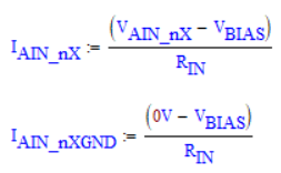
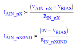
The Datasheet gives the following formula for Analog input current calculation:


Is VIN the differential voltage between AIN_nX and AIN_nXG? Or is it the absolute voltage of each pin against AGND?

Regards
Sebastian

P.S.: When reworking the Datasheet, the unit of the formula could be rethought.
The result is in A.
Because of the value of RIN it is in the range of uA.

  • Hi Sebastian,

    This ADC can only support single-ended input, normally the AIN_nXGND pin is shorted to AGND, so Vin in the formula is the voltage applied to the AIN_nX. 

    We have noticed the unit error in the datasheet, it will be updated in next revision. Thanks.

    Regards,

    Dale

  • Hello Dale,

    for me It is not yet clear which current flows at which pin.

    Are the following formulas/assumption correct?

    VBIAS is the same for both inputs with the tolerance given in the datasheet dependent of the selected input voltage range.

    Is the value for the input resistance RIN the same for both inputs (resistors matched) with the tolerance and temperature drift

    given in the data sheet.

    Or should a separate resistance value with the tolerances and temperature drift given in the data sheet be assumed for each input?

    Is it possible to get a more detailed block diagram of the input stage to get a better understanding of the input?

    Regards, Alexander

  • Hi Alex,

    The formulas are correct. the value of the input resistance Rin for both inputs are same, you can see them (1Mohm) in the device block diagram on the 1st page of the data sheet. All information are shown in the data sheet and we can not share anything else. Let me know if you have any further questions.

    Regards,

    Dale