This thread has been locked.

If you have a related question, please click the "Ask a related question" button in the top right corner. The newly created question will be automatically linked to this question.

ADS127L01EVM: Enquiry about the SPI protocol setup of ADS127L01EVM with Delfino F2833x board.

Part Number: ADS127L01EVM
Other Parts Discussed in Thread: CONTROLSUITE, ADS127L01

Hi. Here i face some issue to set up the SPI communication by ADS127L01EVM (Slave) with Delfino F2833x board (Master), both are TI product.

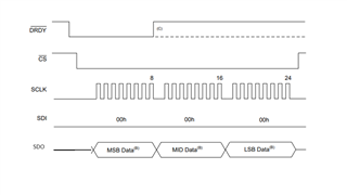
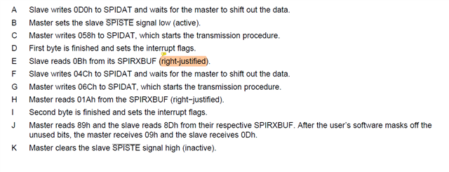
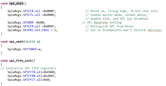
I have referred the spi_loopback code which available in "controlSUITE" and i have done the test of spi command send from Master to slave, but Master is unable to receive any information from slave. I monitor this SPI communication process with digit logic analyzer. Here i attached few pic to illustrate the SPI protocol setting.

Below are few problems that hopefuuly can get support from TI technical teams:

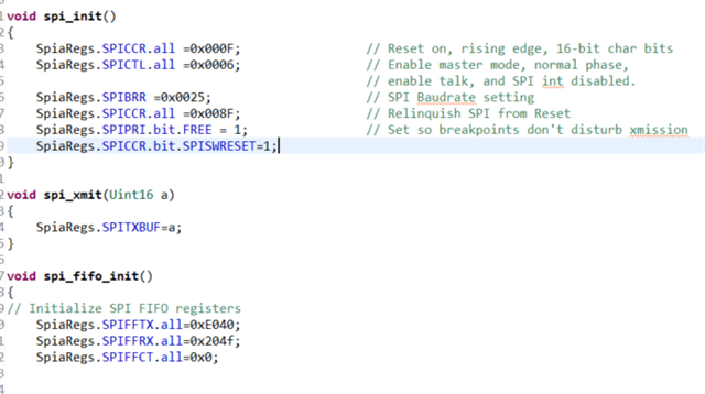
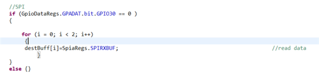
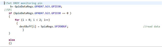
1. For the spi protocol set up with ADS127L01EVM, a input pin is needed to be set for monitoring the DRDY status, may i know is the code i show below is the right way to monitor the status of DRDY pin?

2. There are some spike happen for CS pin although i have set the CS always low in coding. Is there any issue with this phenomena and will it affect the SPI communication process? Pls see the pic attached below.

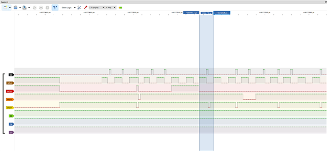
3. Based on the Question 2 pic, the SPIBFF i set is 11 but the SPI SCLK baudrate i measured is 3M Hz which is not the 150M/(SPIBFF+1) = 12.5M Hz. May i know is there any mistake i did for the setting of SPI Baudrate.

  • Hello JH,

    Regarding the specific processor settings, I will need to forward your post to the Delfino support team.

    1.  Yes, this code looks correct.  You need to monitor the /DRDY line, either by software polling or interrupt, and when /DRDY goes low, then start the SPI frame by pulling /CS low, usually with a GPIO pin, and then clocking out the conversion result data.

    2.  Yes, this will cause communications to fail.  CS must remain low during the entire SPI frame.  CS must transition from high to low to start the SPI frame, and held low throughout the frame.  Also, to read conversion data, the MOSI line should be held low during the SPI frame.  Once the conversion data has been read from the ADC, the /CS line should then transition back high to end the frame.

    3.  This is specific to the F2833x processor, and will need addressed by that team.

    Below is what you should measure for a single SPI frame:

    Regards,
    Keith Nicholas 
    Precision ADC Applications

  • Ok. Looking forward to response from Delfino support team where currently the Master (Delfino F2833x board) cnt read any data which send by slave.

    Hope to hear you all soon.

    Thx.

  • Hi JH,

    In terms of part 3 of your post: in your calculations it looks like are using 150MHz which is SYSCLK for F2833x, but the calculation specifies that baud rate = LSPCLK/(BRR+1). Just wanted to see if you could please check to verify what your LSPCLK is at? This can be different from the SYSCLK depending on what dividers are used.

    Regards,

    Allison

  • Ok. Thanks a lot for your response. I have verified it and yes, i have set the LSPCLK accordingly so now for question no.3 is ok.

    By the way, could you please provide support for the Delfino F2833x board SPI setting?

    FYI,Pls look at the SPI setting that i set below for the master mode:

    Currently i face the issue where master (Deflino f2833x) cnt receive the data which sent from slave (ADS127L01EVM), i have ready a code to monitor the drdy pin (GPIO 30) and the master will read the data once the DRDY pin goes low, pls see my code below:

    Now the question is, there are no SCLK pulse from Master and slave select pin did not change to low for activate the CS once the code reach the "master read" code.

    So, may I know is there any other setting/configuration the needed for set up the Master to receive the data from slave.

    Hope you could provide support on this.

    Looking forward to your support. 

  • Hi. Another question related to the SPI setting.

    Is SPISTE pin required for the master mode setting? Or we should set another GPIO pin for the CS (slave control) function?

  • Hi. According to the pic attached below, may i know what is the meaning of the highlighted statement ?

    "Data is output on the SPISIMO pin and latched from the SPISOMI pin"?

  • Hi, just some extra information for you where here i would like read 32b data from the slave (ADS127L01EVM), as per review the SPIRXBUF is just 16b, so is there any setting need to do for make this works?

  • Hi JH,

    Your code for master mode looks to be correct, though I do not think "SpiaRegs.SPICRR.bit.SPISWRESET=1;" is necessary since I believe this bit is already set to 1 when you write "SpiaRegs.SPICRR.all=0x008F;". I think the issue is that the CS pin does need to go low in order for data to be transmitted between master and slave. If F2833x is in master, then it needs to be driving that chip select (CS) pin low before transmission. This is accomplished through the GPIO module of the device by configuring a GPIO to be SPISTE. For example, you can use GPIO Port B MUX 2 to configure GPIO19 or GPIO57 to be SPI-A slave transmit enable (SPISTEA) as shown in Table 1-47. GPIOA MUX and Table 1-48. GPIOB MUX in the device TRM

    When in master mode, you can use a dedicated SPISTE pin or a regular GPIO as the chip-select pin. Please refer to TRM section 9.2.1 SPI Module Signals under Configuring a GPIO to emulate SPISTE for a description of this setup.

    The line Data is output on the SPISIMO pin and latched from the SPISOMI pin refers to the pin locations of where the master sends data (SOMI) and receives data (MISO). The master sends out data to the slave by outputting it on the "slave-in-master-out" pin. The master receives data by "latching" it as it comes in on the slave-out-master-in pin, which just means that the master is capturing and storing the state of bits (0 or 1) when they are received from the slave.

    Regards,

    Allison

  • Hi JH,

    By default after power-up or reset, the ADS127L01 will output 32b data.  You can do this by reading 2x 16b transfers, but you will need to keep the /CS low for the entire transfer frame.  Set /CS pin low, send 16 SCLKs and capture data the MSB data, then send another 16 SCLKS and capture the LSB data.  After the two 16b transfers, set /CS pin high to end the frame.

    Regards,
    Keith

  • Dear Allison Nguyen and Keith Nicholas, thx a lot for the fast response.

    By the way, here i have another question which related to the 9.4.3 Data Communication Example. Pls refer the pic attached below.

    Questions:

    1. May i know what is mean by the "right-justified"?

    2. May i know why in step E, slave read 0Bh and not the 058h which read by Master into itsd SPIDAT?

    3. For the step J, what is means by "After the User's software to masks off the unused bits"? and in the end the salve receive what it send intially at step A?

    Hope you all could help explain this example.

    Thx.

  • Hi JH,

    1. "Left-justified" means that the most significant bit (MSB) is transmitted first and data bits are aligned to the left side of the frame (with any trailing bits filled with zeros. "Right justified" means that the least significant bit (LSB) is transmitted first and data bits are aligned to the right side of the frame (with leading bits filled with zeros). For this system, once SPIDAT has received a complete character, the character is transferred to SPIRXBUF where it can be read. Data that is written to SPIDAT register must be left-justified when written, which means that the data is transmitted MSB first. The MSB when transmitted is shifted into the LSB position of the register, which means it is being stored right-justified in the register. So the data read from SPIRXBUF is thus right-justified.

    2. The master writes 058h to initiate the transmission procedure. Though the value is somewhat arbitrary, it's purpose is to show correct format of communication with the slave. The slave reads 0Bh because of how 058h is written (MSB first). 0Bh is the interpreted data read based upon its formatting (right justified vs. left justified). You can reference these in binary to get a better feel for this as well.

    3. Masking off unused bits refers to setting unused bits (usually with zero) to ensure they are treated as irrelevant and do not affect the target data (the used bits).

    Regards,

    Allison