This thread has been locked.

If you have a related question, please click the "Ask a related question" button in the top right corner. The newly created question will be automatically linked to this question.

LM98640QML-SP: About S/H and CDS modes

Part Number: LM98640QML-SP

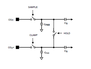
Hello, I'm reading the datasheet of the LM98640QML-SP and I found §8.2.1 a bit confusing: the name of this point is "Sample/Hold Mode", but the figure 29 description mentions "Typical CDS Mode Application Diagram". So what's exactly the configuration shown in Figure 29?

For my particular use I want to use the LM98640QML-SP to measure four 1.5V common-mode / differential outputs from a detector, therefore I would use two LM98640QML-SP and using both OS1/2+ and OS1/2- inputs for each differential output. Can you please clarify what's the application diagram I should follow in my particular case?

Thank you.

  • Hi Carlos, 

    Figure 29 in the datasheet is indeed following Sample and Hold mode but where the reference is VCLP. Hence, they are shorted to VCLP. 

    The device was conceived for single ended input from the image sensors. For your differential input use case, you will have to tweak the register settings a bit. I would highly recommend you to try this on an EVM before proceeding to your final board design. 

    Since your input is differential and 1.5V common mode, you can use Sample and Hold mode. You can DC couple the inputs to OSx+ and OSx- pins (ie. no input coupling capacitors). OSx+ should not be shorted to VCLP and also should not have a bypass capacitor to the ground. 

    OSx- will be recorded on the SAMPLE clock and OSx+ will be recorded on the CLAMP clock (CLPIN Gating Enabled, CLPIN always high). You will have to tweak the SAMPLE clock and CLAMP clock to record your pixel voltages at the right phase.  

    Thanks, 

    Karthik N