This thread has been locked.
If you have a related question, please click the "Ask a related question" button in the top right corner. The newly created question will be automatically linked to this question.
Hello,
I am currently using the TI Delta Sigma Evaluation Software to evaluate the ADS124S08. We are using a full wheatstone bridge made up of 4x strain gauges. The bridge resistance is 1000 ohms. I designed the circuit as per TIs A Basic Guide to Bridge Measurements (ti.com) page 51, 6.5 Four-Wire Resistive Bridge Measurement With a Ratiometric Reference and Current Excitation.
At the moment the evaluation software determines an ENOB of 12.5 bits which i think is quite low for this ADC. I was wondering if there was anyway to improve the performance or if you can spot anything glaringly wrong. .
Adc config:
20 sps
low latency filter
PGA gain of 128
IDAC 1 mA
IDAC current out of AIN3
AIN + = channel 8
AIN- = channel 9
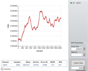
When I run a data analysis at 1 V reference I get the following:
ENOB = 12.5 bits
Is there any way to improve this number? We would ideally like to measure down to at least 1 uV as that lets us resolve 1 uStrain.
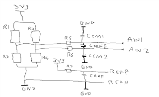
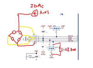
I have set up the ADC eval kit as per below:
I have configured the IDAC on AIN3 to output 1 mA.
I've modified the evaluation kit slightly in order to include a bias resistor of 1.15K between Ref N0 and GND.
I am using AIN8 as positive input and AIN9 as negative.
I measure the correct 1.65 V common mode to both inputs.
Apologies for the poor diagram below but i hope it helps illustrate my circuit.
Any help with this one is appreciated.
Kind regards
Hi Jonathan,
I assume that there is no jumper connected at JP8 and that you have selected the REF0 input pair as the ADC reference. What you end up seeing is a lot of drift. 2048 samples at 20sps is a duration of over 102 seconds. So for long duration testing you should try to isolate strain elements, wiring connections, etc. from thermal gradients.
As far as the noise is concerned you will do slightly better if you use the sinc3 filter as opposed to the low-latency. You can see noise as voltage in the noise table plots in the datasheet. At 20sps and gain of 128 the noise for the low-latency filter is 510nVpp. The noise tables were generated using 512 consecutive samples, so I would suggest limiting your initial measurements to 512 samples to see your performance. If you are not approximating the noise table numbers you can try sinc3 to see if there is any considerable difference. You may have to isolate the EVM from thermal gradients by placing the EVM in some form or box or bag. I have seen great shifts in data due to lab equipment power supply fans.
Best regards,
Bob B
Hi Bob,
Thanks for your help with this one.
I've taken some new measurements now having shielded the electronics and using the sinc3 filter and I am seeing better results. For my voltage excited measurement using 3.3V reference I get 19.6 ENOB and for the current excited measurement I get 17 bits.
I had another question. I am looking at the ADC accuracies and I was hoping for some clarification. As i understand it, we can calibrate out the offset error and gain error using the ADC calibration registers. The ADS124S08 has a gain error of 200 ppm max. Is this 200 ppm of the Full scale range? For instance, If i have a 3.3V reference and using 128 gain I will have a full scale range of 0.0257V does this mean that my gain error is 0.02% of 0.0257 V ? or about 5 uV? Similarly, INL is 15 ppm maximum at PPM FSR - does this work the same way? We want to measure down to 1 uV so it would be helpful to know if this is possible.
Kind regards
Jon
Hi Jon,
It is not clear how you are actually connecting the bridge when voltage exciting. As to the difference in the effective resolution keep in mind that the current excited measurement is using a 1V reference where the LSB value is approximately 1nV where as with a 3.3V reference the LSB value is about 3nV. So when comparing the bit resolution consider not just the ENOB number but what the number represents.
As far as the offset and gain error are concerned, it may be helpful to look at the typical characteristics graphs which will give a better idea of where the error exists relative to temperature in Figures 18-20 of the datasheet. Unless you are operating at the hottest temperatures (greater than 85 deg C) you should not ever see the max values. Gain and INL are specified as ppm of full-scale. So when analyzing error, use an RSS analysis with all units being the same.
Gain error usually dominates over INL and offset but has the greatest impact to the measurement as the input nears full-scale. Deviation from the ideal slope is greatest where the gain error is measured at near full-scale. As the input voltage lowers the deviation from the actual gain slope to the ideal narrows. In many bridge circuits, the actual output voltage relative to full-scale may be 1/4 to 1/8 the full-scale range. So ADC gain error in these situations becomes minimal.
The offset of the ADC can be removed by issuing the SFOCAL which places an internal short within the ADC to 'zero' out the ADC offset. You can also issue SYOCAL (offset) and SYGCAL (gain) calibration commands, but this requires that the user apply a 0V input for offset and a full-scale input for gain calibration. This is difficult to do for bridge measurements and it does not take into account any offset or gain issues with the bridge itself. If the bridge is not temperature compensated, the bridge error may be a larger factor than the ADC.
The other dominant factor is the conversion noise. A delta-sigma ADC is an oversampling converter that increases precision (repeatability of the measurement) by pushing quantization noise into higher frequencies then using a low-pass digital filter to filter the higher frequency content. The end result is displayed in the datasheet noise tables where lower data rates have lower noise where the low-pass filter is most effective. Using the sinc3 filter and 200sps with a gain of 128 shows typical p2p noise at 950nV. So this would be the maximum data rate allowable to come close to 1uV resolution. See datasheet Table 1 and the rightmost column for noise numbers at a gain of 128.
To calibrate the bridge, you can basically use a 2 point calibration to determine the offset and gain slope in point-slope form (y=mx + b). This calibration is done in firmware code. The 'b' value is the ADC code returned for a unloaded bridge (0 input). The slope is just rise/run of the value near or at full-scale output of the bridge.
Best regards,
Bob B
Hi Bob,
Thanks a lot for your feedback.
When voltage exciting I have the top of my bridge connected to 3V3 and the bottom of my bridge connected to ground. I also have my refp0 and refn0 connected to 3v3 and ground respectively. Good point on the different references for both voltage and current excited.
I've had a look at the INL and gain graphs and the numbers do look better than I originally thought. With regards to the gain error, our full scale range is 25.7mV and our maximum bridge output will only be around 2.1 mV. As we are working with less than 10% of full scale range - do you think that gain error is a concern? Looking at the gain error vs temperature graph at a worst case of -10 (our system is deployed outdoors) there is around 60 PPM FSR of gain error this translates to 1.5 uV. Would this 1.5 uV be the worst case at around full scale range?
We are looking at using a gain of 128 and a sampling rate of 20SPS. Looking at the table this looks like a peak to peak noise of 300 nV. Hopefully this will give us a better chance of measuring at a microvolt resolution.
Thanks for the tip on calibrating the bridge - we will try this when it comes to prototyping.
Kind regards
Jon
Hi Jon,
Below is an example of gain error. You can see at the rightmost portion of the graph where the gain error is dramatically different from the ideal with respect to full-scale. From your information we can see that the actual measurement range is less than 1/10th of the full-scale range. Here the actual difference from the ideal is much less.
When calibrating the sensor with respect to the ADC you can match the slope of the gain error to match the ideal. To determine the actual slope you need to apply an input that uses enough of the full-scale range to accurately determine the slope so that you are not calibrating on the noise.
With that said, consider that although the ADC can approach the 300nV resolution, the actual input voltage is a low-level signal and if wiring is such that noise (EMI/RFI) can be picked up the noise of the system may be your dominating source of error.
Best regards,
Bob B
Hi Bob,
Thanks a lot for the info, its appreciated.
I have another couple of questions I hoped you could confirm if that's ok.
I would like to place differential and common mode filtering capacitors on the input of the ADC and the input to the reference. I've followed TIs guide on ratiometric filtering previously for the RTD system. With a sample rate of 20 SPS I believe we choose a differential frequency of 10x that so 200 Hz. We then choose a common mode capacitor that is 1/10th the value of the differential.
As the bridge configuration is slightly different to the RTD I wanted to confirm if i've understood the equations OK.
With the 1000 ohm full active bridge configuration, would the equation for the differential frequency at the inputs be:
F= 1/(2pi *Cdiff(R3+R4+R5+R6)) Where R3 and R4 are the lower 1k bridge resistors and R5 and R6 are the filtering resistors?
Similarly, would the equation for the differential reference frequency be F = 1/(2*pi*Cref*R7) ?
I've attached a quick sketch to illustrate my circuit.
Lastly, as we have a battery operated system we would need to switch the bridge configuration on and off. If we use the integrated low side switch in the ADC - would this have a negative affect on our measurement as there is 1 ohm resistance? Or is this OK if we use a ratiometric ? If we wanted to use the switch would we remove the ground connection to REFN0 (like in the sketch above) and instead have REFN0 connected to ground through AVSS-SW ?
Thanks again for your help Bob.
Kind regards
Jon
Hi Jon,
For a ratiometric measurement you get the most benefit of cancelling out excitation drift from the measurement. With high precision ADCs, it is also desirable that the noise is reduced using the input filters. Attempting to match the filtering between the reference and the analog inputs is a good practice, but in the end a little more difficult than one would expect. The reason being is the reference input filter is relatively static whereas the bridge is dynamic due to the changing nature of the strain elements.
There is also the tolerance of the resistors, so in the end you just need to be in the neighborhood of having similar responses. I would suggest keeping it simple and using R5 and R6 and the differential cap for the ADC inputs computation and balancing with R7 and CREF to have a similar response. I would recommend that CREF be around 100nF and then adjust the rest of the components accordingly.
For excitation break, connect the EXC- from the bridge and REFN0 together (not at analog ground) and connect the AVSS-SW to analog ground. In that way the circuit remains ratiometric and the switch resistance will have no effect on the measurement.
Best regards,
Bob B
Hi Bob,
Thanks for the info, it was very helpful.
Lastly, do you know if the resistances in the bridge affect the frequency equations? Or can we use these 2?
Kind regards
Hi Jon,
Don't try to overthink this too much. You will never be exact in real life systems as all components have tolerances. And yes, the bridge impedance will affect the filter. Any resistance in the current path affects the outcome. Also consider temperature coefficient of the various components. Due to these and other factors that is why I stated the input to the ADC is dynamic and suggested to just get close with the matching.
You can use the fc equations you show (and are in application note SBAA201). For equation 1 I generally eliminate Ccm/2 as Cin will dominate if it is 10x or larger than Ccm.
Just so I am making myself clear, let's back up a step. Let's say there is no Cin in the circuit and you just use Ccm caps for the ADC input. This may all match up nicely with the filter for the reference, but you may see a much noisier ADC result. Why might this happen? If the input filters are not precisely matched to each other (these would be the AIN pins I'm referring to and not the reference) due to component mismatch or tolerance you can see slight differences in the phase between the filters which will end up as a difference voltage to the ADC. With very low level signals and high gain this mismatch could be worse than using no filters at all. So in this case you want the differential filter using Cin to dominate over any potential phase differences.
Now when we match the differential filter to the reference filter, what we are really trying to do is to keep noise of the excitation similar with respect to both the differential input and the reference. Again, this cannot be perfectly matched but you do want it to be close enough so that the filtering of the noise signature of the excitation looks similar for both the reference and ADC inputs.
Hope that helps,
Bob B
Hi Bob,
Thanks for the useful feedback on this.
I've put the following schematic together. We already measure a PT1000 RTD which seems to work well. I've added the strain gauge to another set of inputs as well as some filtering for 200 Hz (i think my calculations are correct..). We will need to switch between references when we take measurements but this should be ok I think (unless you think otherwise). I've connected my VEXC- to my negative reference and plan on connecting them to ground through AVSS-SW.
We do place ESD diodes on the signal lines, these have a leakage current of 0.5 nA at 40 degrees C. I can remove these if the leakage is too high for the measurement, the strain gauge measurement we are trying to take is down to 1 uV.
Can you see anything obviously wrong with this configuration at all? Would be great if you could have a quick look over.
Thanks for your help again, its really appreciated.
Jon3302.ADC.pdf
Hi Jon,
I don't see any issues with the schematic. Using the reference inputs for the separate measurements is fine to do and the reason why multiple reference inputs are provided.
Just one thing I want to mention when using the AVSS-SW switch connection. The switch only automatically opens when the POWERDOWN command is issued. Most likely for your system you will want to manually control the switch by setting the PSW bit. When the PSW bit in the excitation current register 1 (06h) is set to 1, the switch closes. The switch is opened by setting the PSW bit to 0. By default, the switch is open.
Best regards,
Bob B
Hi Bob,
Thanks for your advice and for checking over my schematic.
The plan is to use a 6 wire connection for the strain gauge - this was taken from page 13 of this document https://www.ti.com/lit/an/sbaa532/sbaa532.pdf?ts=170532014372. If the measurement is ratiometric, do the extra 2 wires help at all? If the volt drop affects both the reference and the bridge voltages?
We've also been looking at using a separate N-MOSFET on the VEXC- line. If we were to use a separate MOSFET on the VEXC- line, would this have a negative affect on the measurement at all? Are we better to use the configuration in the schematic in the last post?
I've attached an updated schematic with the alternative solution, please let me know if you think this would be ok.
Appreciate your help.
Hi Jon,
By using the 6-wire over that of the 4-wire, the end result is Kelvin connection for the reference. In this way the excitation of the bridge is being measured at the same point as the connection to the bridge itself. This method of connection improves the accuracy as the measurement does not include and voltage drops of the excitation in the wiring for the reference. It is difficult to predict the overall benefit in your application.
Connecting an external switch is certainly a doable method to control excitation and you should see no negative impact in doing so as shown in your schematic.